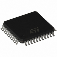
ST72F561J4T6 STMicroelectronics, ST72F561J4T6 Datasheet - Page 161

ST72F561J4T6
Manufacturer Part Number
ST72F561J4T6
Description
IC MCU 8BIT 16K FLASH 44-LQFP
Manufacturer
STMicroelectronics
Series
ST7r
Datasheet
1.ST72F561K6T6.pdf
(265 pages)
Specifications of ST72F561J4T6
Core Processor
ST7
Core Size
8-Bit
Speed
8MHz
Connectivity
CAN, LINSCI, SPI
Peripherals
LVD, POR, PWM, WDT
Number Of I /o
32
Program Memory Size
16KB (16K x 8)
Program Memory Type
FLASH
Ram Size
1K x 8
Voltage - Supply (vcc/vdd)
3.8 V ~ 5.5 V
Data Converters
A/D 16x10b
Oscillator Type
External
Operating Temperature
-40°C ~ 85°C
Package / Case
44-LQFP
Processor Series
ST72F5x
Core
ST7
Data Bus Width
8 bit
Data Ram Size
1 KB
Interface Type
CAN, SCI, SPI
Maximum Clock Frequency
8 MHz
Number Of Programmable I/os
48
Number Of Timers
3
Maximum Operating Temperature
+ 85 C
Mounting Style
SMD/SMT
Development Tools By Supplier
STX-RLINK
Minimum Operating Temperature
- 40 C
On-chip Adc
10 bit, 16 Channel
For Use With
497-8374 - BOARD DEVELOPMENT FOR ST72F561
Lead Free Status / RoHS Status
Lead free / RoHS Compliant
Eeprom Size
-
Lead Free Status / Rohs Status
Details
Available stocks
Company
Part Number
Manufacturer
Quantity
Price
Company:
Part Number:
ST72F561J4T6
Manufacturer:
COILCRAFT
Quantity:
4 000
Company:
Part Number:
ST72F561J4T6
Manufacturer:
STMicroelectronics
Quantity:
10 000
- Current page: 161 of 265
- Download datasheet (10Mb)
LINSCI™ SERIAL COMMUNICATION INTERFACE (LIN Master Only) (Cont’d)
10.8.7 SCI Synchronous Transmission
The SCI transmitter allows the user to control a
one way synchronous serial transmission. The
SCLK pin is the output of the SCI transmitter clock.
No clock pulses are sent to the SCLK pin during
start bit and stop bit. Depending on the state of the
LBCL bit in the SCICR3 register, clock pulses are
or are not be generated during the last valid data
bit (address mark). The CPOL bit in the SCICR3
register allows the user to select the clock polarity,
and the CPHA bit in the SCICR3 register allows
the user to select the phase of the external clock
(see
During idle, preamble and send break, the external
SCLK clock is not activated.
Figure 91. SCI Example of Synchronous and Asynchronous Transmission
Figure
91,
Figure 92
and
SCI
Figure
Output port
SCLK
TDO
RDI
93).
Data out
Data in
Data in
Clock
Enable
These options allow the user to serially control pe-
ripherals which consist of shift registers, without
losing any functions of the SCI transmitter which
can still talk to other SCI receivers. These options
do not affect the SCI receiver which is independ-
ent from the transmitter.
Note: The SCLK pin works in conjunction with the
TDO pin. When the SCI transmitter is disabled (TE
and RE = 0), the SCLK and TDO pins go into high
impedance state.
Note: The LBCL, CPOL and CPHA bits have to be
selected before enabling the transmitter to ensure
that the clock pulses function correctly. These bits
should not be changed while the transmitter is en-
abled.
Asynchronous
(e.g. modem)
Synchronous
(e.g. shift register)
ST72561
161/265
Related parts for ST72F561J4T6
Image
Part Number
Description
Manufacturer
Datasheet
Request
R

Part Number:
Description:
STMicroelectronics [RIPPLE-CARRY BINARY COUNTER/DIVIDERS]
Manufacturer:
STMicroelectronics
Datasheet:

Part Number:
Description:
STMicroelectronics [LIQUID-CRYSTAL DISPLAY DRIVERS]
Manufacturer:
STMicroelectronics
Datasheet:

Part Number:
Description:
BOARD EVAL FOR MEMS SENSORS
Manufacturer:
STMicroelectronics
Datasheet:

Part Number:
Description:
NPN TRANSISTOR POWER MODULE
Manufacturer:
STMicroelectronics
Datasheet:

Part Number:
Description:
TURBOSWITCH ULTRA-FAST HIGH VOLTAGE DIODE
Manufacturer:
STMicroelectronics
Datasheet:

Part Number:
Description:
Manufacturer:
STMicroelectronics
Datasheet:

Part Number:
Description:
DIODE / SCR MODULE
Manufacturer:
STMicroelectronics
Datasheet:

Part Number:
Description:
DIODE / SCR MODULE
Manufacturer:
STMicroelectronics
Datasheet:

Part Number:
Description:
Search -----> STE16N100
Manufacturer:
STMicroelectronics
Datasheet:

Part Number:
Description:
Search ---> STE53NA50
Manufacturer:
STMicroelectronics
Datasheet:

Part Number:
Description:
NPN Transistor Power Module
Manufacturer:
STMicroelectronics
Datasheet:

Part Number:
Description:
DIODE / SCR MODULE
Manufacturer:
STMicroelectronics
Datasheet:


