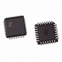
Z86E3016VSG Zilog, Z86E3016VSG Datasheet - Page 12

Z86E3016VSG
Manufacturer Part Number
Z86E3016VSG
Description
IC MICROCONTROLLER 4K 28-PLCC
Manufacturer
Zilog
Series
Z8®r
Datasheet
1.Z86E4001ZDV.pdf
(64 pages)
Specifications of Z86E3016VSG
Core Processor
Z8
Core Size
8-Bit
Speed
16MHz
Peripherals
POR, WDT
Number Of I /o
24
Program Memory Size
4KB (4K x 8)
Program Memory Type
OTP
Ram Size
237 x 8
Voltage - Supply (vcc/vdd)
3.5 V ~ 5.5 V
Oscillator Type
Internal
Operating Temperature
0°C ~ 70°C
Package / Case
28-PLCC
Processor Series
Z86E3xx
Core
Z8
Data Bus Width
8 bit
Data Ram Size
237 B
Maximum Clock Frequency
16 MHz
Number Of Programmable I/os
24
Number Of Timers
2
Operating Supply Voltage
3.5 V to 5.5 V
Maximum Operating Temperature
+ 70 C
Mounting Style
SMD/SMT
Development Tools By Supplier
Z86CCP01ZEM, Z86CCP00ZAC, Z86C3000ZAC
Minimum Operating Temperature
0 C
Lead Free Status / RoHS Status
Lead free / RoHS Compliant
Eeprom Size
-
Data Converters
-
Connectivity
-
Lead Free Status / Rohs Status
Details
Available stocks
Company
Part Number
Manufacturer
Quantity
Price
Z86E30/E31/E40
Z8 4K OTP Microcontroller
ABSOLUTE MAXIMUM RATINGS
Ambient Temperature under Bias
Storage Temperature
Voltage on any Pin with Respect to V
Voltage on V
Voltage on XTAL1 and RESET Pins with Respect to V
Total Power Dissipation
Maximum Allowable Current out of V
Maximum Allowable Current into V
Maximum Allowable Current into an Input Pin [Note 3]
Maximum Allowable Current into an Open-Drain Pin [Note 4]
Maximum Allowable Output Current Sinked by Any I/O Pin
Maximum Allowable Output Current Sourced by Any I/O Pin
Maximum Allowable Output Current Sinked by RESET Pin
Notes:
Stresses greater than those listed under Absolute Maxi-
mum Ratings may cause permanent damage to the de-
vice. This is a stress rating only; functional operation of the
device at any condition above those indicated in the oper-
ational sections of these specifications is not implied. Ex-
posure to absolute maximum rating conditions for an ex-
tended period may affect device reliability.
STANDARD TEST CONDITIONS
The characteristics listed below apply for standard test
conditions as noted. All voltages are referenced to
Ground. Positive current flows into the referenced pin
(Test Load).
12
1. This applies to all pins except XTAL pins and where otherwise noted.
2. There is no input protection diode from pin to V
3. This excludes XTAL pins.
4. Device pin is not at an output Low state.
DD
Pin with Respect to V
Parameter
DD
SS
SS
SS
[Note 1]
DD
P R E L I M I N A R Y
.
SS
[Note 2]
Total power dissipation should not exceed 1.2 W for the
package. Power dissipation is calculated as follows:
Total Power Dissipation = V
+ sum of [ (V
+ sum of (V
From Output
Under Test
–600
–600
–0.6
–0.3
–0.6
Min
–40
–65
0L
DD
Figure 13. Test Load Diagram
x I
– V
0L
)
OH
) x I
OH
V
+105
+150
+600
+600
3 mA
DD
Max
1.21
DD
220
180
+7
+7
25
25
]
+1
x [ I
DD
– (sum of I
DS97Z8X0502
150 pF
Units
mA
mA
mA
mA
W
C
C
V
V
V
A
A
OH
) ]
Zilog


