Z86E3016VSG Zilog, Z86E3016VSG Datasheet - Page 44
Z86E3016VSG
Manufacturer Part Number
Z86E3016VSG
Description
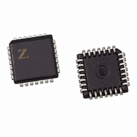
IC MICROCONTROLLER 4K 28-PLCC
Manufacturer
Zilog
Series
Z8®r
Datasheet
1.Z86E4001ZDV.pdf
(64 pages)
Specifications of Z86E3016VSG
Core Processor
Z8
Core Size
8-Bit
Speed
16MHz
Peripherals
POR, WDT
Number Of I /o
24
Program Memory Size
4KB (4K x 8)
Program Memory Type
OTP
Ram Size
237 x 8
Voltage - Supply (vcc/vdd)
3.5 V ~ 5.5 V
Oscillator Type
Internal
Operating Temperature
0°C ~ 70°C
Package / Case
28-PLCC
Processor Series
Z86E3xx
Core
Z8
Data Bus Width
8 bit
Data Ram Size
237 B
Maximum Clock Frequency
16 MHz
Number Of Programmable I/os
24
Number Of Timers
2
Operating Supply Voltage
3.5 V to 5.5 V
Maximum Operating Temperature
+ 70 C
Mounting Style
SMD/SMT
Development Tools By Supplier
Z86CCP01ZEM, Z86CCP00ZAC, Z86C3000ZAC
Minimum Operating Temperature
0 C
Lead Free Status / RoHS Status
Lead free / RoHS Compliant
Eeprom Size
-
Data Converters
-
Connectivity
-
Lead Free Status / Rohs Status
Details
Available stocks
Company
Part Number
Manufacturer
Quantity
Price


FUNCTIONAL DESCRIPTION (Continued)
Z86E30/E31/E40
Z8 4K OTP Microcontroller
Stop-Mode Recovery Delay Select (D5). The 5 ms RE-
SET delay after Stop-Mode Recovery is disabled by pro-
gramming this bit to a zero. A “1” in this bit will cause a 5
ms RESET delay after Stop-Mode Recovery. The default
condition of this bit is 1. If the fast wake up mode is select-
ed, the Stop-Mode Recovery source needs to be kept ac-
tive for at least 5TpC.
Stop-Mode Recovery Level Select (D6). A “1” in this bit
defines that a high level on any one of the recovery sourc-
es wakes the MCU from STOP Mode. A 0 defines low level
recovery. The default value is 0.
Cold or Warm Start (D7). This bit is set by the device
upon entering STOP Mode. A “0” in this bit indicates that
the device has been reset by POR (cold). A “1” in this bit
indicates the device was awakened by a SMR source
(warm).
Stop-Mode Recovery Register 2 (SMR2). This register
contains additional Stop-Mode Recovery sources. When
the Stop-Mode Recovery sources are selected in this reg-
ister then SMR Register. Bits D2, D3, and D4 must be 0.
D1
0
0
1
Watch-Dog Timer Mode Register (WDTMR). The WDT
is a retriggerable one-shot timer that resets the Z8 if it
reaches its terminal count. The WDT is disabled after Pow-
er-On Reset and initially enabled by executing the WDT in-
struction and refreshed on subsequent executions of the
WDT instruction. The WDT is driven either by an on-board
RC oscillator or an external oscillator from XTAL1 pin. The
44
D4
SMR:10
0
0
0
0
1
1
1
1
D0
0
1
0
Table 12. Stop-Mode Recovery Source
D3
0
0
1
1
0
0
1
1
Operation
Description of Action
POR and/or external reset recovery
Logical AND of P20 through P23
Logical AND of P20 through P27
D2
0
1
0
1
0
1
0
1
POR recovery only
P30 transition
P31 transition (Not in analog
mode)
P32 transition (Not in analog
mode)
P33 transition (Not in analog
mode)
P27 transition
Logical NOR of Port 2 bits 0–3
Logical NOR of Port 2 bits 0–7
SMR Source selection
P R E L I M I N A R Y
POR clock source is selected with bit 4 of the WDT regis-
ter.
Note: Execution of the WDT instruction affects the Z (Ze-
ro), S (Sign), and V (Overflow) flags.
WDT Time-Out Period (D0 and D1). Bits 0 and 1 control
a tap circuit that determines the time-out periods that can
be obtained (Table 13). The default value of D0 and D1
are 1 and 0, respectively.
Notes:
WDT During HALT Mode (D2). This bit determines
whether or not the WDT is active during HALT Mode. A “1”
indicates that the WDT is active during HALT. A “0” dis-
ables the WDT in HALT Mode. The default value is “1”.
WDT During STOP Mode (D3). This bit determines
whether or not the WDT is active during STOP mode. A “1”
indicates active during STOP. A “0” disables the WDT dur-
ing STOP Mode. This is applicable only when the WDT
clock source is the internal RC oscillator.
Clock Source For WDT (D4). This bit determines which
oscillator source is used to clock the internal POR and
WDT counter chain. If the bit is a 1, the internal RC oscil-
lator is bypassed and the POR and WDT clock source is
driven from the external pin, XTAL1, and the WDT is
stopped in STOP Mode. The default configuration of this
bit is 0, which selects the RC oscillator.
Permanent WDT. When this feature is enabled, the WDT
is enabled after reset and will operate in Run and Halt
Mode. The control bits in the WDTMR do not affect the
WDT operation. If the clock source of the WDT is the inter-
nal RC oscillator, then the WDT will run in STOP mode. If
the clock source of the WDT is the XTAL1 pin, then the
WDT will not run in STOP mode.
Note: WDT time-out in STOP Mode will not reset
SMR,SMR2,PCON, WDTMR, P2M, P3M, Ports 2 & 3 Data
Registers.
WDTMR Register Accessibility. The WDTMR register is
accessible only during the first 60 internal system clock
*The default setting is 10 ms.
D1
0
0
1
1
Table 13. Time-out Period of WDT
D0
0
1
0
1
Time-out of
the Internal
RC OSC
10 ms*
20 ms
80 ms
5 ms
DS97Z8X0502
Time-out of
the System
2048 SCLK
256 SCLK*
128 SCLK
512 SCLK
Clock
Zilog
Related parts for Z86E3016VSG
Image
Part Number
Description
Manufacturer
Datasheet
Request
R

Part Number:
Description:
Communication Controllers, ZILOG INTELLIGENT PERIPHERAL CONTROLLER (ZIP)
Manufacturer:
Zilog, Inc.
Datasheet:

Part Number:
Description:
KIT DEV FOR Z8 ENCORE 16K TO 64K
Manufacturer:
Zilog
Datasheet:

Part Number:
Description:
KIT DEV Z8 ENCORE XP 28-PIN
Manufacturer:
Zilog
Datasheet:

Part Number:
Description:
DEV KIT FOR Z8 ENCORE 8K/4K
Manufacturer:
Zilog
Datasheet:

Part Number:
Description:
KIT DEV Z8 ENCORE XP 28-PIN
Manufacturer:
Zilog
Datasheet:

Part Number:
Description:
DEV KIT FOR Z8 ENCORE 4K TO 8K
Manufacturer:
Zilog
Datasheet:
Part Number:
Description:
CMOS Z8 microcontroller. ROM 16 Kbytes, RAM 256 bytes, speed 16 MHz, 32 lines I/O, 3.0V to 5.5V
Manufacturer:
Zilog, Inc.
Datasheet:
Part Number:
Description:
Low-cost microcontroller. 512 bytes ROM, 61 bytes RAM, 8 MHz
Manufacturer:
Zilog, Inc.
Datasheet:
Part Number:
Description:
Z8 4K OTP Microcontroller
Manufacturer:
Zilog, Inc.
Datasheet:
Part Number:
Description:
CMOS SUPER8 ROMLESS MCU
Manufacturer:
Zilog, Inc.
Datasheet:
Part Number:
Description:
SL1866 CMOSZ8 OTP Microcontroller
Manufacturer:
Zilog, Inc.
Datasheet:
Part Number:
Description:
SL1866 CMOSZ8 OTP Microcontroller
Manufacturer:
Zilog, Inc.
Datasheet:
Part Number:
Description:
OTP (KB) = 1, RAM = 125, Speed = 12, I/O = 14, 8-bit Timers = 2, Comm Interfaces Other Features = Por, LV Protect, Voltage = 4.5-5.5V
Manufacturer:
Zilog, Inc.
Datasheet:
Part Number:
Description:
Manufacturer:
Zilog, Inc.
Datasheet: