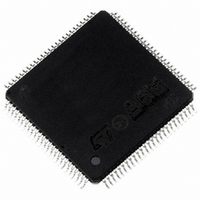
ST10R172LT1 STMicroelectronics, ST10R172LT1 Datasheet - Page 17

ST10R172LT1
Manufacturer Part Number
ST10R172LT1
Description
MCU 16BIT ROMLESS LV 100TQFP
Manufacturer
STMicroelectronics
Series
ST10r
Datasheet
1.ST10R172LT6.pdf
(68 pages)
Specifications of ST10R172LT1
Core Processor
ST10
Core Size
16-Bit
Speed
50MHz
Connectivity
EBI/EMI, SSP, UART/USART
Peripherals
POR, PWM, WDT
Number Of I /o
77
Program Memory Type
ROMless
Ram Size
1K x 8
Voltage - Supply (vcc/vdd)
3 V ~ 3.6 V
Oscillator Type
Internal
Operating Temperature
0°C ~ 70°C
Package / Case
100-TQFP, 100-VQFP
Controller Family/series
ST10
No. Of I/o's
77
Ram Memory Size
1KB
Cpu Speed
50MHz
No. Of Timers
5
Embedded Interface Type
SPI, USART
No. Of Pwm Channels
1
Rohs Compliant
Yes
Processor Series
ST10R1x
Core
ST10
Data Bus Width
16 bit
Data Ram Size
1 KB
Interface Type
SSP, USART
Maximum Clock Frequency
50 MHz
Number Of Programmable I/os
77
Number Of Timers
5
Maximum Operating Temperature
+ 70 C
Mounting Style
SMD/SMT
Minimum Operating Temperature
0 C
On-chip Adc
8 bit
Lead Free Status / RoHS Status
Lead free / RoHS Compliant
Eeprom Size
-
Program Memory Size
-
Data Converters
-
Lead Free Status / Rohs Status
In Transition
Available stocks
Company
Part Number
Manufacturer
Quantity
Price
Company:
Part Number:
ST10R172LT1
Manufacturer:
TI
Quantity:
101
Company:
Part Number:
ST10R172LT1
Manufacturer:
STMicroelectronics
Quantity:
10 000
Company:
Part Number:
ST10R172LT1VJ029CNX
Manufacturer:
ST
Quantity:
50
Company:
Part Number:
ST10R172LT1VJ052JNX
Manufacturer:
ST
Quantity:
34
6
The ST10R172L provides up to 77 I/O lines organized into 7 input/output ports and one input
port. All port lines are bit-addressable, and all input/output lines are individually (bit-wise)
programmable as inputs or outputs by direction registers. The I/O ports are true bidirectional
ports which are switched to high impedance state when configured as inputs. The output
drivers of three I/O ports can be configured (pin by pin) for push/pull operation or open-drain
operation by control registers. During the internal reset, all port pins are configured as inputs.
All port lines have programmable alternate input or output functions associated with them.
PORT0 and PORT1 may be used as address and data lines when accessing external
memory, while Port 4 outputs the additional segment address bits A23/19/17...A16 in systems
where segmentation is enabled to access more than 64 KBytes of memory. Port 6 provides
optional bus arbitration signals (BREQ, HLDA, HOLD) and chip select signals. Port 3 includes
alternate functions of timers, serial interfaces, the optional bus control signal BHE and the
system clock output (CLKOUT). Port 5 is used for timer control signals. Port 2 lines can be
used as fast external interrupt lines. Port 7 includes alternate function for the PWM signal. All
port lines that are not used for these alternate functions may be used as general purpose I/O
lines.
7
All external memory accesses are performed by the on-chip External Bus Controller which
can be programmed either to single chip mode when no external memory is required, or to the
following external memory access modes:
In the demultiplexed bus modes, addresses are output on PORT1 and data is input/output on
PORT0/P0L, respectively. In the multiplexed bus modes both addresses and data use PORT0
for input/output.
Memory cycle time, memory tri-state time, length of ALE and read write delay are
programmable so that a wide range of different memory types and external peripherals can be
used. Up to 4 independent address windows can be defined (via ADDRSELx / BUSCONx
register pairs) to access different resources with different bus characteristics. These address
windows are arranged hierarchically where BUSCON4 overrides BUSCON3 etc. All accesses
to locations not covered by these 4 address windows are controlled by BUSCON0. Up to 5
external CS signals (4 windows plus default) can be generated to reduce external glue logic.
Access to very slow memories is supported by the READY function.
A HOLD/HLDA protocol is available for bus arbitration so that external resources can be
shared with other bus masters. In slave mode, the slave controller can be connected to an-
other master controller without glue logic. For applications which require less than 16 MBytes
16-bit data, demultiplexed
16-bit data, multiplexed
8-bit data, multiplexed
8-bit data, demultiplexed
PARALLEL PORTS
EXTERNAL BUS CONTROLLER
16-/18-/20-/24-bit addresses
16-/18-/20-/24-bit addresses
16-/18-/20-/24-bit addresses
16-/18-/20-/24-bit addresses
ST10R172L - PARALLEL PORTS
17/68
1


