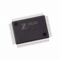
Z16F2810FI20EG Zilog, Z16F2810FI20EG Datasheet - Page 63

Z16F2810FI20EG
Manufacturer Part Number
Z16F2810FI20EG
Description
IC ZNEO MCU FLASH 128K 80QFP
Manufacturer
Zilog
Series
Encore!® ZNEOr
Datasheet
1.Z16F2800100ZCOG.pdf
(388 pages)
Specifications of Z16F2810FI20EG
Core Processor
ZNEO
Core Size
16-Bit
Speed
20MHz
Connectivity
I²C, IrDA, LIN, SPI, UART/USART
Peripherals
Brown-out Detect/Reset, DMA, POR, PWM, WDT
Number Of I /o
60
Program Memory Size
128KB (128K x 8)
Program Memory Type
FLASH
Ram Size
4K x 8
Voltage - Supply (vcc/vdd)
2.7 V ~ 3.6 V
Data Converters
A/D 12x10b
Oscillator Type
Internal
Operating Temperature
-40°C ~ 105°C
Package / Case
80-BQFP
Data Bus Width
16 bit
Data Ram Size
4 B
Interface Type
ESPI, I2C, UART
Maximum Clock Frequency
20 MHz
Number Of Programmable I/os
60
Number Of Timers
4
Operating Supply Voltage
2.7 V to 3.6 V
Maximum Operating Temperature
+ 105 C
Mounting Style
SMD/SMT
Minimum Operating Temperature
- 40 C
On-chip Adc
10 bit, 12 Channel
For Use With
770-1003 - ISP 4PORT FOR ZILOG ZNEO MCU269-4537 - DEV KIT FOR Z16F ZNEO
Lead Free Status / RoHS Status
Lead free / RoHS Compliant
Eeprom Size
-
Lead Free Status / Rohs Status
Details
Available stocks
Company
Part Number
Manufacturer
Quantity
Price
- Current page: 63 of 388
- Download datasheet (22Mb)
PS022008-0810
External Interface Timing
Table 14. External Interface Timing for a Write Operation - Normal Mode
Parameter
T
T
T
T
T
T
T
T
T
T
T
T
T
T
1
2
3
4
5
6
7
8
9
10
11
12
13
14
External Interface Write Timing - Normal Mode
The following sections describe the external interface timing.
Figure 11
performing a Write operation. In
generator is configured to provide 1 Wait state during Write operations. The external
WAIT input pin is generating an additional Wait period. Also in
assumed that the chip select (CS) signal has been configured for active Low operation.
Though the internal system clock is not provided as an external signal, it provides a useful
reference for control signal events. Note that at the completion of a Write cycle, the
de-assertion of the WR signal is fed back from the pin and used on chip to control the
de-assertion of the data, CS, address and byte enable signals to assure proper timing of the
data hold.
Abbreviation
SYS CLK Rise to Address Valid Delay
WR Rise to Address Output Hold Time
SYS CLK Rise to Data Valid Delay
WR Rise to Data Output Hold Time
SYS CLK Rise to CS Assertion Delay
WR Rise to CS Deassertion Hold Time
SYS CLK Rise to WR Assertion Delay
SYS CLK Rise to WR Deassertion Hold Time
WAIT Input Pin Assertion to XIN Rise Setup Time
WAIT Input Pin Deassertion to XIN Rise Setup Time
SYS CLK Rise to DMAACK Assertion Delay
SYS CLK Rise to DMAACK Deassertion Hold Time
SYS CLK Rise to BHEN or BLEN Assertion Delay
WR Rise to BHEN or BLEN Deassertion Hold Time
on page 49 and
Table 14
P R E L I M I N A R Y
Figure 11
provide timing information for the external interface
on page 49, it is assumed that the Wait state
Minimum
3
3
3
3
1
1
3
3
Figure 11
Product Specification
Delay (ns)
ZNEO
Tclk +10
External Interface
Maximum
on page 49, it is
Z16F Series
10
10
10
10
10
48
Related parts for Z16F2810FI20EG
Image
Part Number
Description
Manufacturer
Datasheet
Request
R

Part Number:
Description:
Communication Controllers, ZILOG INTELLIGENT PERIPHERAL CONTROLLER (ZIP)
Manufacturer:
Zilog, Inc.
Datasheet:

Part Number:
Description:
KIT DEV FOR Z8 ENCORE 16K TO 64K
Manufacturer:
Zilog
Datasheet:

Part Number:
Description:
KIT DEV Z8 ENCORE XP 28-PIN
Manufacturer:
Zilog
Datasheet:

Part Number:
Description:
DEV KIT FOR Z8 ENCORE 8K/4K
Manufacturer:
Zilog
Datasheet:

Part Number:
Description:
KIT DEV Z8 ENCORE XP 28-PIN
Manufacturer:
Zilog
Datasheet:

Part Number:
Description:
DEV KIT FOR Z8 ENCORE 4K TO 8K
Manufacturer:
Zilog
Datasheet:

Part Number:
Description:
CMOS Z8 microcontroller. ROM 16 Kbytes, RAM 256 bytes, speed 16 MHz, 32 lines I/O, 3.0V to 5.5V
Manufacturer:
Zilog, Inc.
Datasheet:

Part Number:
Description:
Low-cost microcontroller. 512 bytes ROM, 61 bytes RAM, 8 MHz
Manufacturer:
Zilog, Inc.
Datasheet:

Part Number:
Description:
Z8 4K OTP Microcontroller
Manufacturer:
Zilog, Inc.
Datasheet:

Part Number:
Description:
CMOS SUPER8 ROMLESS MCU
Manufacturer:
Zilog, Inc.
Datasheet:

Part Number:
Description:
SL1866 CMOSZ8 OTP Microcontroller
Manufacturer:
Zilog, Inc.
Datasheet:

Part Number:
Description:
SL1866 CMOSZ8 OTP Microcontroller
Manufacturer:
Zilog, Inc.
Datasheet:

Part Number:
Description:
OTP (KB) = 1, RAM = 125, Speed = 12, I/O = 14, 8-bit Timers = 2, Comm Interfaces Other Features = Por, LV Protect, Voltage = 4.5-5.5V
Manufacturer:
Zilog, Inc.
Datasheet:

Part Number:
Description:
Manufacturer:
Zilog, Inc.
Datasheet:


