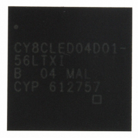
CY8CLED04D01-56LTXI Cypress Semiconductor Corp, CY8CLED04D01-56LTXI Datasheet - Page 33

CY8CLED04D01-56LTXI
Manufacturer Part Number
CY8CLED04D01-56LTXI
Description
IC POWERPSOC 4CH 1A 56VQFN
Manufacturer
Cypress Semiconductor Corp
Series
PowerPSoC® CY8CLEDr
Datasheet
1.CY8CLED03D02-56LTXI.pdf
(47 pages)
Specifications of CY8CLED04D01-56LTXI
Package / Case
56-VQFN Exposed Pad, 56-HVQFN, 56-SQFN, 56-DHVQFN
Core Processor
M8C
Core Size
8-Bit
Speed
24MHz
Connectivity
DALI, DMX512, I²C, IrDA, SPI, UART/USART
Peripherals
LED, LVD, POR, PWM, WDT
Number Of I /o
14
Program Memory Size
16KB (16K x 8)
Program Memory Type
FLASH
Ram Size
1K x 8
Voltage - Supply (vcc/vdd)
4.75 V ~ 5.25 V
Oscillator Type
Internal
Operating Temperature
-40°C ~ 85°C
Operating Supply Voltage
7 V to 32 V
Maximum Supply Current
50 mA
Maximum Operating Temperature
+ 85 C
Mounting Style
SMD/SMT
Minimum Operating Temperature
- 40 C
Lead Free Status / RoHS Status
Lead free / RoHS Compliant
For Use With
428-2882 - KIT STARTER POWERPSOC LIGHTING428-2281 - KIT EVAL POWERPSOC LIGHTING428-2271 - KIT EVAL COLOR-LOCK428-2270 - KIT STARTER DEMO LIGHTING770-1000 - ISP 4PORT FOR CYPRESS PSOC MCU
Eeprom Size
-
Data Converters
-
Lead Free Status / Rohs Status
Lead free / RoHS Compliant
Other names
428-2279
Available stocks
Company
Part Number
Manufacturer
Quantity
Price
Company:
Part Number:
CY8CLED04D01-56LTXI
Manufacturer:
HONEYWELL
Quantity:
1 200
Part Number:
CY8CLED04D01-56LTXI
Manufacturer:
CYPRESS/赛普拉斯
Quantity:
20 000
15.9 Power Peripheral Reference DAC Specification
The following table lists guaranteed maximum and minimum specifications for the voltage and temperature ranges: 4.75V to 5.25V
and T
Table 15-16. Reference DAC DC Specifications
Table 15-17. Reference DAC AC Specifications
15.10 Power Peripheral Built-in Switching Regulator
The following table lists guaranteed maximum and minimum specifications for the voltage and temperature ranges: 4.75V to 5.25V
and T
Table 15-18. Built-in Switching Regulator DC Specifications
Document Number: 001-46319 Rev. *E
I
INL
DNL
A
OS
V
V
t
t
V
V
V
V
I
I
I
I
R
Line
Load
PSRR
E
SDAC
SETTLE
STARTUP
LOAD
S,BSR
SB,HV
INRUSH
ERROR
DACFS
DACMM
REGIN
REGOUT
RIPPLE
UVLO
BSR
DS(ON),PFET
Symbol
Symbol
Symbol
ERROR
REG
REG
J
J
≤ 115
≤ 115
o
o
C. Typical parameters apply to 5V at 25°C. These are for design guidance only.
C. Typical parameters apply to 5V at 25°C. These are for design guidance only.
Output settling time to 0.5 LSB of final value
Startup time to within 0.5 LSB of final value
Input Supply Voltage Range
Output Voltage Range
Output Ripple
Under Voltage Lockout Voltage
DC Output Current -Active Mode
Supply Current - Built-in Switching
Regulator
Standby Current (High Voltage)
Inrush Current
PFET Drain to Source ON resistance
Line Regulation
Load Regulation
Power Supply Rejection Ratio
Built-in Switching Regulator Efficiency
Supply Current - Reference DAC
Integral Non Linearity
Differential Non Linearity
Gain Error
Offset Error
Fullscale Voltage - Reference DAC
Fullscale Voltage Mismatch (Pair of
Reference DACs - Even and Odd)
Description
Description
Description
0.01
Min
4.8
5.5
Min
-1.5
-0.5
Min
80
7
–
–
–
–
–
–
–
–
-1
-5
-7
–
–
–
–
–
–
–
–
Typ
5.0
2.5
-60
Typ
Typ
–
–
–
–
–
–
–
1
1
–
–
–
–
–
–
–
–
–
–
–
–
–
–
CY8CLED04G01, CY8CLED03G01
CY8CLED04D01, CY8CLED04D02
CY8CLED03D01, CY8CLED03D02
Max
100
250
250
5.2
6.5
1.2
Max
32
600
Max
10.5
1.5
0.5
2.6
1.3
12
4
–
–
–
–
–
10
1
5
7
1
7
Units
Units
Units
mV
mA
mA
mV
mV
LSB
LSB
LSB
LSB
LSB
LSB
LSB
LSB
LSB
LSB
μA
dB
%
Ω
μA
V
V
V
A
μs
μs
See
page 25
Does not include V
V
V
I
V
250 mA
V
f
V
LOAD
RIPPLE
Mode 0 and Mode1
Mode 0
Mode 1
Mode 0 and Mode1
Mode 0
Mode 1
Mode 0 and Mode1
Mode 0
Mode 1
Mode 0
Mode 1
Mode 0 and Mode1
Mode 0 and Mode1
REGIN
REGIN
REGIN
RIPPLE
REGIN
Absolute Maximum Ratings
= 250 mA, V
< V
> V
= 1 kHz to 10 kHz
= 24V, I
= 24V, I
= 0.2*V
UVLO
UVLO
Notes
Notes
Notes
LOAD
LOAD
REGIN,
: Power Down Mode
: Active Mode
REGIN
RIPPLE
= 2.5 mA to
= 250 mA
Page 33 of 47
= 7V to 32V
on
[+] Feedback


