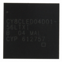
CY8CLED04D01-56LTXI Cypress Semiconductor Corp, CY8CLED04D01-56LTXI Datasheet - Page 37

CY8CLED04D01-56LTXI
Manufacturer Part Number
CY8CLED04D01-56LTXI
Description
IC POWERPSOC 4CH 1A 56VQFN
Manufacturer
Cypress Semiconductor Corp
Series
PowerPSoC® CY8CLEDr
Datasheet
1.CY8CLED03D02-56LTXI.pdf
(47 pages)
Specifications of CY8CLED04D01-56LTXI
Package / Case
56-VQFN Exposed Pad, 56-HVQFN, 56-SQFN, 56-DHVQFN
Core Processor
M8C
Core Size
8-Bit
Speed
24MHz
Connectivity
DALI, DMX512, I²C, IrDA, SPI, UART/USART
Peripherals
LED, LVD, POR, PWM, WDT
Number Of I /o
14
Program Memory Size
16KB (16K x 8)
Program Memory Type
FLASH
Ram Size
1K x 8
Voltage - Supply (vcc/vdd)
4.75 V ~ 5.25 V
Oscillator Type
Internal
Operating Temperature
-40°C ~ 85°C
Operating Supply Voltage
7 V to 32 V
Maximum Supply Current
50 mA
Maximum Operating Temperature
+ 85 C
Mounting Style
SMD/SMT
Minimum Operating Temperature
- 40 C
Lead Free Status / RoHS Status
Lead free / RoHS Compliant
For Use With
428-2882 - KIT STARTER POWERPSOC LIGHTING428-2281 - KIT EVAL POWERPSOC LIGHTING428-2271 - KIT EVAL COLOR-LOCK428-2270 - KIT STARTER DEMO LIGHTING770-1000 - ISP 4PORT FOR CYPRESS PSOC MCU
Eeprom Size
-
Data Converters
-
Lead Free Status / Rohs Status
Lead free / RoHS Compliant
Other names
428-2279
Available stocks
Company
Part Number
Manufacturer
Quantity
Price
Company:
Part Number:
CY8CLED04D01-56LTXI
Manufacturer:
HONEYWELL
Quantity:
1 200
Part Number:
CY8CLED04D01-56LTXI
Manufacturer:
CYPRESS/赛普拉斯
Quantity:
20 000
15.12 PSoC Core Operational Amplifier Specifications
The following table lists guaranteed maximum and minimum specifications for the voltage and temperature ranges: 4.75V to 5.25V
and T
The Operational Amplifier is a component of both the Analog Continuous Time PSoC blocks and the Analog Switched Capacitor PSoC
blocks. The guaranteed specifications are measured in the Analog Continuous Time PSoC block.
Table 15-23. Operational Amplifier DC Specifications
Document Number: 001-46319 Rev. *E
V
TCV
I
C
V
G
V
V
I
PSRR
EBOA
SOA
Symbol
OSOA
CMOA
OHIGHOA
OLOWOA
INOA
OLOA
OSOA
J
OA
≤ 115°C. Typical parameters apply to 5V at 25°C. These are for design guidance only.
Input Offset Voltage (absolute value)
Power = Low, Opamp Bias = High
Power = Medium, Opamp Bias = High
Power = High, Opamp Bias = High
Average Input Offset Voltage Drift
Input Leakage Current (Port 0 analog pins)
Input Capacitance (Port 0 analog pins)
Common Mode Voltage Range
Common Mode Voltage Range (high power
or high opamp bias)
Open Loop Gain
Power = Low, Opamp Bias = High
Power = Medium, Opamp Bias = High
Power = High, Opamp Bias = High
High Output Voltage Swing (internal signals)
Power = Low, Opamp Bias = High
Power = Medium, Opamp Bias = High
Power = High, Opamp Bias = High
Low Output Voltage Swing (internal signals)
Power = Low, Opamp Bias = High
Power = Medium, Opamp Bias = High
Power = High, Opamp Bias = High
Supply Current (including associated Analog
Output Buffer)
Power = Low, Opamp Bias = Low
Power = Low, Opamp Bias = High
Power = Medium, Opamp Bias = Low
Power = Medium, Opamp Bias = High
Power = High, Opamp Bias = Low
Power = High, Opamp Bias = High
Supply Voltage Rejection Ratio
Description
VDD - 0.2
VDD - 0.2
VDD - 0.5
Min
0.0
0.5
60
60
80
52
–
–
–
–
–
–
–
–
–
–
–
–
–
–
1200
2400
4600
Typ
400
500
800
1.6
1.3
1.2
7.0
4.5
20
80
–
–
–
–
–
–
–
–
–
–
–
CY8CLED04G01, CY8CLED03G01
CY8CLED04D01, CY8CLED04D02
CY8CLED03D01, CY8CLED03D02
VDD - 0.5
VDD
1000
1600
3200
6400
Max
35.0
800
900
7.5
0.2
0.2
0.5
9.5
10
8
–
–
–
–
–
–
–
–
μV/°C
Units
mV
mV
mV
pA
pF
dB
dB
dB
μA
μA
μA
μA
μA
μA
dB
V
V
V
V
V
V
V
V
Gross tested to 1 μA.
T
The common-mode input voltage
range is measured through an
analog output buffer. The specifi-
cation includes the limitations
imposed by the characteristics of
the analog output buffer.
VSS ≤ VIN ≤ (VDD - 2.25) or (VDD
- 1.25V) ≤ VIN ≤ VDD.
J
= 25°C.
Notes
Page 37 of 47
[+] Feedback


