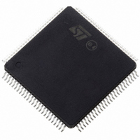
ST10F269Z2T3 STMicroelectronics, ST10F269Z2T3 Datasheet - Page 181

ST10F269Z2T3
Manufacturer Part Number
ST10F269Z2T3
Description
MCU 16BIT 256KBIT FLASH 144-TQFP
Manufacturer
STMicroelectronics
Series
ST10r
Datasheet
1.ST10F269Z2Q3.pdf
(184 pages)
Specifications of ST10F269Z2T3
Core Processor
ST10
Core Size
16-Bit
Speed
40MHz
Connectivity
CAN, EBI/EMI, SSC, UART/USART
Peripherals
POR, PWM, WDT
Number Of I /o
111
Program Memory Size
256KB (256K x 8)
Program Memory Type
FLASH
Ram Size
12K x 8
Voltage - Supply (vcc/vdd)
4.5 V ~ 5.5 V
Data Converters
A/D 16x10b
Oscillator Type
Internal
Operating Temperature
-40°C ~ 125°C
Package / Case
144-TQFP, 144-VQFP
Processor Series
ST10F26x
Core
ST10
Data Bus Width
16 bit
Data Ram Size
12 KB
Interface Type
CAN, SSC, USART
Maximum Clock Frequency
40 MHz
Number Of Programmable I/os
111
Number Of Timers
5
Maximum Operating Temperature
+ 125 C
Mounting Style
SMD/SMT
Minimum Operating Temperature
- 40 C
On-chip Adc
10 bit, 16 Channel
Lead Free Status / RoHS Status
Lead free / RoHS Compliant
Eeprom Size
-
Lead Free Status / Rohs Status
Details
Available stocks
Company
Part Number
Manufacturer
Quantity
Price
Company:
Part Number:
ST10F269Z2T3
Manufacturer:
LITTLEFUSE
Quantity:
1 000
Company:
Part Number:
ST10F269Z2T3
Manufacturer:
STMicroelectronics
Quantity:
10 000
1 - DESCRIPTION
This Errata sheet describes the functional and electrical problems known in the D revision of the
ST10F269Zxxx.
The revision number can be found in the third line on the ST10F269 package. It looks like: ’xxxxxxxxx D’
where "D" identifies the revision number.
2 - FUNCTIONAL PROBLEMS
The following malfunctions are known in this step:
2.1 - PWRDN.1 - Execution of PWRDN Instruction
When instruction PWRDN is executed while pin NMI is at a high level (if PWRDCFG bit is clear in
SYSCON register) or while at least one of the port 2 pins used to exit from power-down mode (if PWRD-
CFG bit is set in SYSCON register) is at the active level, power down mode is not entered, and the
PWRDN instruction is ignored.
However, under the conditions described below, the PWRDN instruction is not ignored, and no further
instructions are fetched from external memory, i.e. the CPU is in a quasi-idle state.
This problem only occurs in the following situations:
a) The instructions following the PWRDN instruction are located in an external memory, and a multi-
b) The instruction preceeding the PWRDN instruction writes to external memory or an XPeripheral
Note: The on-chip peripherals are still working correctly, in particular the Watchdog Timer, if not disabled,
resets the device upon an overflow. Interrupts and PEC transfers, however, cannot be processed. In case
NMI is asserted low while the device is in this quasi-idle state, power-down mode is entered.
No problem occurs if the NMI pin is low (if PWRDCFG = 0) or if all P2 pins used to exit from power-down
mode are at inactive level (if PWRDCFG = 1): the chip normally enters powerdown mode.
Workaround:
Ensure that no instruction that writes to external memory or an XPeripheral preceeds the PWRDN
instruction, otherwise insert a NOP instruction in front of PWRDN. When a multiplexed bus with memory
tristate wait state is used, the PWRDN instruction must be executed from internal RAM or XRAM.
September 2003
plexed bus configuration with memory tristate waitstate (bit MT-TCx = 0) is used.
Or
(XRAM,CAN), and the instructions following the PWRDN instruction are located in external memory.
In this case, the problem occurs for any bus configuration.
LIMITATIONS AND CORRECTIONS
ERRATA SHEET
ST10F269Zxxx-D
181/184


