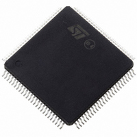
ST10F269Z2T3 STMicroelectronics, ST10F269Z2T3 Datasheet - Page 27

ST10F269Z2T3
Manufacturer Part Number
ST10F269Z2T3
Description
MCU 16BIT 256KBIT FLASH 144-TQFP
Manufacturer
STMicroelectronics
Series
ST10r
Datasheet
1.ST10F269Z2Q3.pdf
(184 pages)
Specifications of ST10F269Z2T3
Core Processor
ST10
Core Size
16-Bit
Speed
40MHz
Connectivity
CAN, EBI/EMI, SSC, UART/USART
Peripherals
POR, PWM, WDT
Number Of I /o
111
Program Memory Size
256KB (256K x 8)
Program Memory Type
FLASH
Ram Size
12K x 8
Voltage - Supply (vcc/vdd)
4.5 V ~ 5.5 V
Data Converters
A/D 16x10b
Oscillator Type
Internal
Operating Temperature
-40°C ~ 125°C
Package / Case
144-TQFP, 144-VQFP
Processor Series
ST10F26x
Core
ST10
Data Bus Width
16 bit
Data Ram Size
12 KB
Interface Type
CAN, SSC, USART
Maximum Clock Frequency
40 MHz
Number Of Programmable I/os
111
Number Of Timers
5
Maximum Operating Temperature
+ 125 C
Mounting Style
SMD/SMT
Minimum Operating Temperature
- 40 C
On-chip Adc
10 bit, 16 Channel
Lead Free Status / RoHS Status
Lead free / RoHS Compliant
Eeprom Size
-
Lead Free Status / Rohs Status
Details
Available stocks
Company
Part Number
Manufacturer
Quantity
Price
Company:
Part Number:
ST10F269Z2T3
Manufacturer:
LITTLEFUSE
Quantity:
1 000
Company:
Part Number:
ST10F269Z2T3
Manufacturer:
STMicroelectronics
Quantity:
10 000
ST10F269
5.5.2 - Basic Flash Access Control
When accessing the Flash all command write addresses have to be located within the active Flash
memory space. The active Flash memory space is that logical address range which is covered by the
Flash after mapping. When using data page pointer (DPP) for addressing the Flash, make sure that
address bit A15 and A14 of the command addresses are reflected in both LSBs of the selected data page
pointer (A15 - DPPx.1 and A14 - DPPx.0).
In case of the command write addresses, address bit A14, A15 and above are don’t care. Thus, command
writes can be performed by only using one DPP register. This allow to have a more simple and compact
application software.
Another - advantageous - possibility is to use the extended segment instruction for addressing.
Note: The direct addressing mode is not allowed for write access to the Flash address/command
The following basic instruction sequences show examples for different addressing possibilities.
Principle example of address generation for Flash commands and registers:
When using data page pointer (DPP0 is this example)
MOV
MOV
MOV
MOV
When using the extended segment instruction:
MOV
MOV
MOV
EXTS
MOV
register. Be aware that the C compiler may use this kind of addressing. For write accesses to
Flash module always the indirect addressing mode has to be selected.
DPP0,#08h
Rw
Rw
[Rw
Rw
Rw
Rw
Rw
[Rw
m
n
m
o
n
n
,#ADDRESS
,#DATA
,#ADDRESS
,#DATA
,#SEGMENT
,#LENGTH
m
m
],Rw
],Rw
n
o
;adjust data page pointers according to the
;addresses: DPP0 is used in this example, thus
;ADDRESS must have A14 and A15 bit set to ‘0’.
;ADDRESS could be a dedicated command sequence
;address 2AA8h, 1554h ... ) or the Flash write
;address
;DATA could be a dedicated command sequence data
;(xxA0h,xx80h ... ) or data to be programmed
;indirect addressing
;ADDRESS could be a dedicated command sequence
;address (2AA8h, 1554h ... ) or the Flash write
;address
;DATA could be a dedicated command sequence data
;(xxA0h,xx80h ... ) or data to be programmed
;the value of SEGMENT represents the segment
;number and could be 0, 1, 2, 3 or 4 (depending
;on sector mapping) for 256KByte Flash.
;the value of Rwn determines the 8-bit segment
;valid for the corresponding data access for any
;long or indirect address in the following(s)
;instruction(s). LENGTH defines the number of
;the effected instruction(s) and has to be a value
;between 1...4
;indirect addressing with segment number from
;EXTS
5 - INTERNAL FLASH MEMORY
27/184


