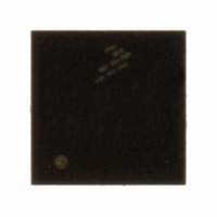
MC9S08QG8MFQE Freescale Semiconductor, MC9S08QG8MFQE Datasheet - Page 30

MC9S08QG8MFQE
Manufacturer Part Number
MC9S08QG8MFQE
Description
IC MCU 8K FLASH 8-DFN
Manufacturer
Freescale Semiconductor
Series
HCS08r
Datasheet
1.MC9S08QG8CDTER.pdf
(314 pages)
Specifications of MC9S08QG8MFQE
Core Processor
HCS08
Core Size
8-Bit
Speed
20MHz
Connectivity
I²C, SCI, SPI
Peripherals
LVD, POR, PWM, WDT
Number Of I /o
4
Program Memory Size
8KB (8K x 8)
Program Memory Type
FLASH
Ram Size
512 x 8
Voltage - Supply (vcc/vdd)
1.8 V ~ 3.6 V
Data Converters
A/D 4x10b
Oscillator Type
Internal
Operating Temperature
-40°C ~ 125°C
Package / Case
8-DFN
Processor Series
S08QG
Core
HCS08
Data Bus Width
8 bit
Data Ram Size
512 B
Interface Type
I2C, SCI, SPI
Maximum Clock Frequency
20 MHz
Number Of Programmable I/os
4
Number Of Timers
1
Maximum Operating Temperature
+ 125 C
Mounting Style
SMD/SMT
3rd Party Development Tools
EWS08
Development Tools By Supplier
DEMO9S08QG8E
Minimum Operating Temperature
- 40 C
On-chip Adc
10 bit, 4 Channel
For Use With
DEMO9S08QG8E - BOARD DEMO FOR MC9S08QG8
Lead Free Status / RoHS Status
Lead free / RoHS Compliant
Eeprom Size
-
Lead Free Status / Rohs Status
Details
- Current page: 30 of 314
- Download datasheet (6Mb)
Chapter 2 External Signal Description
2.2.4
During a power-on-reset (POR) or background debug force reset (see
Force Reset Register
mode select pin. Immediately after any reset, the pin functions as the background pin and can be used for
background debug communication. When enabled as the BKGD/MS pin (BKGDPE = 1), an internal
pullup device is automatically enabled.
The background debug communication function is enabled when BKGDPE in SOPT1 is set. BKGDPE is
set following any reset of the MCU and must be cleared to use the PTA4/ACMPO/BKGD/MS pin’s
alternative pin functions.
If nothing is connected to this pin, the MCU will enter normal operating mode at the rising edge of the
internal reset after a POR or force BDC reset. If a debug system is connected to the 6-pin standard
background debug header, it can hold BKGD/MS low during a POR or immediately after issuing a
background debug force reset, which will force the MCU to active background mode.
The BKGD pin is used primarily for background debug controller (BDC) communications using a custom
protocol that uses 16 clock cycles of the target MCU’s BDC clock per bit time. The target MCU’s BDC
clock could be as fast as the maximum bus clock rate, so there must never be any significant capacitance
connected to the BKGD/MS pin that could interfere with background serial communications.
Although the BKGD pin is a pseudo open-drain pin, the background debug communication protocol
provides brief, actively driven, high speedup pulses to ensure fast rise times. Small capacitances from
cables and the absolute value of the internal pullup device play almost no role in determining rise and fall
times on the BKGD pin.
2.2.5
The MC9S08QG8/4 series of MCUs support up to 12 general-purpose I/O pins, 1 input-only pin, and 1
output-only pin, which are shared with on-chip peripheral functions (timers, serial I/O, ADC, keyboard
interrupts, etc.). On each MC9S08QG8/4 device, there is one input-only and one output-only port pin.
When a port pin is configured as a general-purpose output or a peripheral uses the port pin as an output,
software can select one of two drive strengths and enable or disable slew rate control. When a port pin is
configured as a general-purpose input or a peripheral uses the port pin as an input, software can enable a
pullup device.
For information about controlling these pins as general-purpose I/O pins, see the
Input/Output
see the appropriate chapter referenced in
Immediately after reset, all pins that are not output-only are configured as high-impedance
general-purpose inputs with internal pullup devices disabled. After reset, the output-only port function is
not enabled but is configured for low output drive strength with slew rate control enabled. The PTA4 pin
defaults to BKGD/MS on any reset.
28
Background / Mode Select (BKGD/MS)
General-Purpose I/O and Peripheral Ports
Control.”
(SBDFR),” for more information), the PTA4/ACMPO/BKGD/MS pin functions as a
For information about how and when on-chip peripheral systems use these pins,
MC9S08QG8 and MC9S08QG4 Data Sheet, Rev. 5
Table
2-2.
5.8.3, “System Background Debug
Chapter 6, “Parallel
Freescale Semiconductor
Related parts for MC9S08QG8MFQE
Image
Part Number
Description
Manufacturer
Datasheet
Request
R
Part Number:
Description:
Manufacturer:
Freescale Semiconductor, Inc
Datasheet:
Part Number:
Description:
Manufacturer:
Freescale Semiconductor, Inc
Datasheet:
Part Number:
Description:
Manufacturer:
Freescale Semiconductor, Inc
Datasheet:
Part Number:
Description:
Manufacturer:
Freescale Semiconductor, Inc
Datasheet:
Part Number:
Description:
Manufacturer:
Freescale Semiconductor, Inc
Datasheet:
Part Number:
Description:
Manufacturer:
Freescale Semiconductor, Inc
Datasheet:
Part Number:
Description:
Manufacturer:
Freescale Semiconductor, Inc
Datasheet:
Part Number:
Description:
Manufacturer:
Freescale Semiconductor, Inc
Datasheet:
Part Number:
Description:
Manufacturer:
Freescale Semiconductor, Inc
Datasheet:
Part Number:
Description:
Manufacturer:
Freescale Semiconductor, Inc
Datasheet:
Part Number:
Description:
Manufacturer:
Freescale Semiconductor, Inc
Datasheet:
Part Number:
Description:
Manufacturer:
Freescale Semiconductor, Inc
Datasheet:
Part Number:
Description:
Manufacturer:
Freescale Semiconductor, Inc
Datasheet:
Part Number:
Description:
Manufacturer:
Freescale Semiconductor, Inc
Datasheet:
Part Number:
Description:
Manufacturer:
Freescale Semiconductor, Inc
Datasheet:


