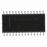
MC908JL16CDWE Freescale Semiconductor, MC908JL16CDWE Datasheet - Page 165

MC908JL16CDWE
Manufacturer Part Number
MC908JL16CDWE
Description
IC MCU 16K FLASH 8MHZ 28-SOIC
Manufacturer
Freescale Semiconductor
Series
HC08r
Datasheet
1.MC908JL16CFJER.pdf
(230 pages)
Specifications of MC908JL16CDWE
Core Processor
HC08
Core Size
8-Bit
Speed
8MHz
Connectivity
I²C, SCI
Peripherals
LED, LVD, POR, PWM
Number Of I /o
23
Program Memory Size
16KB (16K x 8)
Program Memory Type
FLASH
Ram Size
512 x 8
Voltage - Supply (vcc/vdd)
2.7 V ~ 5.5 V
Data Converters
A/D 12x10b
Oscillator Type
Internal
Operating Temperature
-40°C ~ 85°C
Package / Case
28-SOIC (7.5mm Width)
Controller Family/series
HC08
No. Of I/o's
23
Ram Memory Size
512Byte
Cpu Speed
8MHz
No. Of Timers
2
Embedded Interface Type
I2C, SCI
Rohs Compliant
Yes
Processor Series
HC08JL
Core
HC08
Data Bus Width
8 bit
Data Ram Size
512 B
Interface Type
SCI
Maximum Clock Frequency
16 MHz
Number Of Programmable I/os
23
Number Of Timers
4
Operating Supply Voltage
2.7 V to 5.5 V
Maximum Operating Temperature
+ 85 C
Mounting Style
SMD/SMT
Development Tools By Supplier
FSICEBASE, DEMO908JL16E, M68CBL05CE
Minimum Operating Temperature
- 40 C
On-chip Adc
10 bit, 12 Channel
For Use With
DEMO908JL16E - BOARD DEMO FOR MC908JL16
Lead Free Status / RoHS Status
Lead free / RoHS Compliant
Eeprom Size
-
Lead Free Status / Rohs Status
Details
Available stocks
Company
Part Number
Manufacturer
Quantity
Price
Company:
Part Number:
MC908JL16CDWE
Manufacturer:
Freescale
Quantity:
2 865
Part Number:
MC908JL16CDWE
Manufacturer:
FREESCALE
Quantity:
20 000
- Current page: 165 of 230
- Download datasheet (2Mb)
Chapter 14
Low-Voltage Inhibit (LVI)
14.1 Introduction
This section describes the low-voltage inhibit module (LVI), which monitors the voltage on the V
and generates a reset when the V
14.2 Features
Features of the LVI module include the following:
14.3 Functional Description
Figure 14-1
contains a bandgap reference circuit and comparator. Setting LVI disable bit (LVID) disables the LVI to
monitor V
LVI module should take actions.
The LVI module generates one output signal:
LVI Reset — an reset signal will be generated to reset the CPU when V
point.
Freescale Semiconductor
•
•
Selectable LVI trip voltage
Selectable LVI circuit disable
DD
shows the structure of the LVI module. The LVI is enabled after a reset. The LVI module
voltage. The LVI trip voltage selection bits (LVIT1, LVIT0) determine at which V
LVIT1
DETECTOR
LOW V
V
DD
DD
LVIT0
V
V
Figure 14-1. LVI Module Block Diagram
DD
DD
> LVI
< LVI
DD
MC68HC908JL16 Data Sheet, Rev. 1.1
TRIP
TRIP
voltage falls to the LVI trip (LVI
= 0
= 1
LVID
TRIP
DD
) voltage.
drops to below the set trip
LVI RESET
DD
level the
DD
pin
165
Related parts for MC908JL16CDWE
Image
Part Number
Description
Manufacturer
Datasheet
Request
R
Part Number:
Description:
Manufacturer:
Freescale Semiconductor, Inc
Datasheet:
Part Number:
Description:
Manufacturer:
Freescale Semiconductor, Inc
Datasheet:
Part Number:
Description:
Manufacturer:
Freescale Semiconductor, Inc
Datasheet:
Part Number:
Description:
Manufacturer:
Freescale Semiconductor, Inc
Datasheet:
Part Number:
Description:
Manufacturer:
Freescale Semiconductor, Inc
Datasheet:
Part Number:
Description:
Manufacturer:
Freescale Semiconductor, Inc
Datasheet:
Part Number:
Description:
Manufacturer:
Freescale Semiconductor, Inc
Datasheet:
Part Number:
Description:
Manufacturer:
Freescale Semiconductor, Inc
Datasheet:
Part Number:
Description:
Manufacturer:
Freescale Semiconductor, Inc
Datasheet:
Part Number:
Description:
Manufacturer:
Freescale Semiconductor, Inc
Datasheet:
Part Number:
Description:
Manufacturer:
Freescale Semiconductor, Inc
Datasheet:
Part Number:
Description:
Manufacturer:
Freescale Semiconductor, Inc
Datasheet:
Part Number:
Description:
Manufacturer:
Freescale Semiconductor, Inc
Datasheet:
Part Number:
Description:
Manufacturer:
Freescale Semiconductor, Inc
Datasheet:
Part Number:
Description:
Manufacturer:
Freescale Semiconductor, Inc
Datasheet:


