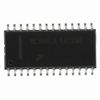
MC908JL16CDWE Freescale Semiconductor, MC908JL16CDWE Datasheet - Page 86

MC908JL16CDWE
Manufacturer Part Number
MC908JL16CDWE
Description
IC MCU 16K FLASH 8MHZ 28-SOIC
Manufacturer
Freescale Semiconductor
Series
HC08r
Datasheet
1.MC908JL16CFJER.pdf
(230 pages)
Specifications of MC908JL16CDWE
Core Processor
HC08
Core Size
8-Bit
Speed
8MHz
Connectivity
I²C, SCI
Peripherals
LED, LVD, POR, PWM
Number Of I /o
23
Program Memory Size
16KB (16K x 8)
Program Memory Type
FLASH
Ram Size
512 x 8
Voltage - Supply (vcc/vdd)
2.7 V ~ 5.5 V
Data Converters
A/D 12x10b
Oscillator Type
Internal
Operating Temperature
-40°C ~ 85°C
Package / Case
28-SOIC (7.5mm Width)
Controller Family/series
HC08
No. Of I/o's
23
Ram Memory Size
512Byte
Cpu Speed
8MHz
No. Of Timers
2
Embedded Interface Type
I2C, SCI
Rohs Compliant
Yes
Processor Series
HC08JL
Core
HC08
Data Bus Width
8 bit
Data Ram Size
512 B
Interface Type
SCI
Maximum Clock Frequency
16 MHz
Number Of Programmable I/os
23
Number Of Timers
4
Operating Supply Voltage
2.7 V to 5.5 V
Maximum Operating Temperature
+ 85 C
Mounting Style
SMD/SMT
Development Tools By Supplier
FSICEBASE, DEMO908JL16E, M68CBL05CE
Minimum Operating Temperature
- 40 C
On-chip Adc
10 bit, 12 Channel
For Use With
DEMO908JL16E - BOARD DEMO FOR MC908JL16
Lead Free Status / RoHS Status
Lead free / RoHS Compliant
Eeprom Size
-
Lead Free Status / Rohs Status
Details
Available stocks
Company
Part Number
Manufacturer
Quantity
Price
Company:
Part Number:
MC908JL16CDWE
Manufacturer:
Freescale
Quantity:
2 865
Part Number:
MC908JL16CDWE
Manufacturer:
FREESCALE
Quantity:
20 000
- Current page: 86 of 230
- Download datasheet (2Mb)
Serial Communications Interface (SCI)
7.3 Pin Name Conventions
The generic names of the SCI I/O pins are:
The SCI I/O (input/output) lines are dedicated pins for the SCI module.
and the generic names of the SCI I/O pins.
The generic pin names appear in the text of this section.
7.4 Functional Description
Figure 7-2
communication among the MCU and remote devices, including other MCUs. The transmitter and receiver
of the SCI operate independently, although they use the same baud rate generator. During normal
operation, the CPU monitors the status of the SCI, writes the data to be transmitted, and processes
received data. The baud rate clock source for the SCI is the bus clock.
86
$0013
$0014
$0015
$0016
$0017
$0018
$0019
Addr.
•
•
RxD (receive data)
TxD (transmit data)
SCI Baud Rate Register
shows the structure of the SCI module. The SCI allows full-duplex, asynchronous, NRZ serial
Register Name
SCI Control Register 1
SCI Control Register 2
SCI Control Register 3
SCI Status Register 1
SCI Status Register 2
SCI Data Register
1. Position of MMIIC module pins (SDA and SCL) is user selectable using CONFIG2
option bit. Refer to
MOR)
MMIIC is enabled and using PTD7/PTD6 for its pins. For more information on MMIIC,
(see
Generic Pin Names:
(SCDR)
(SCBR)
(SCC1)
(SCC2)
(SCC3)
(SCS1)
(SCS2)
Chapter 8 Multi-Master IIC Interface
Full Pin Names:
for additional information. SDA/SCL have priority over the RxD/TxD when
Reset:
Reset:
Reset:
Reset:
Reset:
Reset:
Reset:
Read:
Read:
Read:
Read:
Read:
Read:
Read:
Write:
Write:
Write:
Write:
Write:
Write:
Write:
Figure 7-1. SCI I/O Register Summary
Chapter 3 Configuration and Mask Option Registers (CONFIG and
Table 7-1. Pin Name Conventions
LOOPS
SCTIE
SCTE
Bit 7
MC68HC908JL16 Data Sheet, Rev. 1.1
R8
R7
T7
U
0
0
1
0
0
0
= Unimplemented
ENSCI
TCIE
TC
R6
T8
T6
U
6
0
0
1
0
0
0
PTD7/RxD/SDA
DMARE
(MMIIC)).
SCRIE
TXINV
SCRF
SCP1
RxD
R5
T5
5
0
0
0
0
0
0
R = Reserved
DMATE
(1)
Unaffected by reset
SCP0
IDLE
ILIE
R4
T4
M
4
0
0
0
0
0
0
WAKE
PTD6/TxD/SCL
ORIE
Table 7-1
OR
TE
R3
T3
R
3
0
0
0
0
0
0
TxD
U = Unaffected
SCR2
NEIE
ILTY
RE
NF
R2
T2
2
0
0
0
0
0
0
shows the full names
Freescale Semiconductor
(1)
SCR1
RWU
FEIE
PEN
BKF
FE
R1
T1
1
0
0
0
0
0
0
SCR0
PEIE
Bit 0
PTY
SBK
RPF
PE
R0
T0
0
0
0
0
0
0
Related parts for MC908JL16CDWE
Image
Part Number
Description
Manufacturer
Datasheet
Request
R
Part Number:
Description:
Manufacturer:
Freescale Semiconductor, Inc
Datasheet:
Part Number:
Description:
Manufacturer:
Freescale Semiconductor, Inc
Datasheet:
Part Number:
Description:
Manufacturer:
Freescale Semiconductor, Inc
Datasheet:
Part Number:
Description:
Manufacturer:
Freescale Semiconductor, Inc
Datasheet:
Part Number:
Description:
Manufacturer:
Freescale Semiconductor, Inc
Datasheet:
Part Number:
Description:
Manufacturer:
Freescale Semiconductor, Inc
Datasheet:
Part Number:
Description:
Manufacturer:
Freescale Semiconductor, Inc
Datasheet:
Part Number:
Description:
Manufacturer:
Freescale Semiconductor, Inc
Datasheet:
Part Number:
Description:
Manufacturer:
Freescale Semiconductor, Inc
Datasheet:
Part Number:
Description:
Manufacturer:
Freescale Semiconductor, Inc
Datasheet:
Part Number:
Description:
Manufacturer:
Freescale Semiconductor, Inc
Datasheet:
Part Number:
Description:
Manufacturer:
Freescale Semiconductor, Inc
Datasheet:
Part Number:
Description:
Manufacturer:
Freescale Semiconductor, Inc
Datasheet:
Part Number:
Description:
Manufacturer:
Freescale Semiconductor, Inc
Datasheet:
Part Number:
Description:
Manufacturer:
Freescale Semiconductor, Inc
Datasheet:


