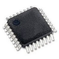
MCHC908GR8AMFAER Freescale Semiconductor, MCHC908GR8AMFAER Datasheet - Page 167

MCHC908GR8AMFAER
Manufacturer Part Number
MCHC908GR8AMFAER
Description
IC MCU 8K FLASH 8MHZ 32-LQFP
Manufacturer
Freescale Semiconductor
Series
HC08r
Specifications of MCHC908GR8AMFAER
Core Processor
HC08
Core Size
8-Bit
Speed
8MHz
Connectivity
SCI, SPI
Peripherals
LVD, POR, PWM
Number Of I /o
21
Program Memory Size
7.5KB (7.5K x 8)
Program Memory Type
FLASH
Ram Size
384 x 8
Voltage - Supply (vcc/vdd)
2.7 V ~ 5.5 V
Data Converters
A/D 6x8b
Oscillator Type
Internal
Operating Temperature
-40°C ~ 125°C
Package / Case
32-LQFP
Controller Family/series
HC08
No. Of I/o's
21
Ram Memory Size
384Byte
Cpu Speed
8MHz
No. Of Timers
2
Embedded Interface Type
I2C, SCI, SPI
Rohs Compliant
Yes
Processor Series
HC08G
Core
HC08
Data Bus Width
8 bit
Data Ram Size
384 B
Interface Type
SCI, SPI
Maximum Clock Frequency
8.2 MHz
Number Of Programmable I/os
21
Number Of Timers
3
Maximum Operating Temperature
+ 125 C
Mounting Style
SMD/SMT
Development Tools By Supplier
FSICEBASE, DEMO908GZ60E, M68CBL05CE, M68EML08GPGTE
Minimum Operating Temperature
- 40 C
On-chip Adc
8 bit, 6 Channel
Lead Free Status / RoHS Status
Lead free / RoHS Compliant
Eeprom Size
-
Lead Free Status / Rohs Status
Details
Available stocks
Company
Part Number
Manufacturer
Quantity
Price
Company:
Part Number:
MCHC908GR8AMFAER
Manufacturer:
Freescale Semiconductor
Quantity:
10 000
- Current page: 167 of 292
- Download datasheet (4Mb)
14.8.3 ESCI Control Register 3
ESCI control register 3 (SCC3):
R8 — Received Bit 8
T8 — Transmitted Bit 8
ORIE — Receiver Overrun Interrupt Enable Bit
NEIE — Receiver Noise Error Interrupt Enable Bit
FEIE — Receiver Framing Error Interrupt Enable Bit
PEIE — Receiver Parity Error Interrupt Enable Bit
Freescale Semiconductor
•
•
When the ESCI is receiving 9-bit characters, R8 is the read-only ninth bit (bit 8) of the received
character. R8 is received at the same time that the SCDR receives the other 8 bits.
When the ESCI is receiving 8-bit characters, R8 is a copy of the eighth bit (bit 7). Reset has no effect
on the R8 bit.
When the ESCI is transmitting 9-bit characters, T8 is the read/write ninth bit (bit 8) of the transmitted
character. T8 is loaded into the transmit shift register at the same time that the SCDR is loaded into
the transmit shift register. Reset clears the T8 bit.
This read/write bit enables ESCI error CPU interrupt requests generated by the receiver overrun bit,
OR. Reset clears ORIE.
This read/write bit enables ESCI error CPU interrupt requests generated by the noise error bit, NE.
Reset clears NEIE.
This read/write bit enables ESCI error CPU interrupt requests generated by the framing error bit, FE.
Reset clears FEIE.
This read/write bit enables ESCI receiver CPU interrupt requests generated by the parity error bit, PE.
Reset clears PEIE.
1 = ESCI error CPU interrupt requests from OR bit enabled
0 = ESCI error CPU interrupt requests from OR bit disabled
1 = ESCI error CPU interrupt requests from NE bit enabled
0 = ESCI error CPU interrupt requests from NE bit disabled
1 = ESCI error CPU interrupt requests from FE bit enabled
0 = ESCI error CPU interrupt requests from FE bit disabled
1 = ESCI error CPU interrupt requests from PE bit enabled
0 = ESCI error CPU interrupt requests from PE bit disabled
Stores the ninth ESCI data bit received and the ninth ESCI data bit to be transmitted.
Enables these interrupts:
–
–
–
–
Receiver overrun
Noise error
Framing error
Parity error
Address:
Reset:
Read:
Write:
MC68HC908GT16 • MC68HC908GT8 • MC68HC08GT16 Data Sheet, Rev. 5.0
$0015
Bit 7
R8
U
Figure 14-12. ESCI Control Register 3 (SCC3)
= Unimplemented
T8
6
0
R
5
0
R
R
4
0
= Reserved
ORIE
3
0
U = Unaffected
NEIE
2
0
FEIE
1
0
PEIE
Bit 0
0
I/O Registers
167
Related parts for MCHC908GR8AMFAER
Image
Part Number
Description
Manufacturer
Datasheet
Request
R
Part Number:
Description:
Manufacturer:
Freescale Semiconductor, Inc
Datasheet:
Part Number:
Description:
Manufacturer:
Freescale Semiconductor, Inc
Datasheet:
Part Number:
Description:
Manufacturer:
Freescale Semiconductor, Inc
Datasheet:
Part Number:
Description:
Manufacturer:
Freescale Semiconductor, Inc
Datasheet:
Part Number:
Description:
Manufacturer:
Freescale Semiconductor, Inc
Datasheet:
Part Number:
Description:
Manufacturer:
Freescale Semiconductor, Inc
Datasheet:
Part Number:
Description:
Manufacturer:
Freescale Semiconductor, Inc
Datasheet:
Part Number:
Description:
Manufacturer:
Freescale Semiconductor, Inc
Datasheet:
Part Number:
Description:
Manufacturer:
Freescale Semiconductor, Inc
Datasheet:
Part Number:
Description:
Manufacturer:
Freescale Semiconductor, Inc
Datasheet:
Part Number:
Description:
Manufacturer:
Freescale Semiconductor, Inc
Datasheet:
Part Number:
Description:
Manufacturer:
Freescale Semiconductor, Inc
Datasheet:
Part Number:
Description:
Manufacturer:
Freescale Semiconductor, Inc
Datasheet:
Part Number:
Description:
Manufacturer:
Freescale Semiconductor, Inc
Datasheet:
Part Number:
Description:
Manufacturer:
Freescale Semiconductor, Inc
Datasheet:


