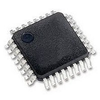
MCHC908GR8AMFAER Freescale Semiconductor, MCHC908GR8AMFAER Datasheet - Page 235

MCHC908GR8AMFAER
Manufacturer Part Number
MCHC908GR8AMFAER
Description
IC MCU 8K FLASH 8MHZ 32-LQFP
Manufacturer
Freescale Semiconductor
Series
HC08r
Specifications of MCHC908GR8AMFAER
Core Processor
HC08
Core Size
8-Bit
Speed
8MHz
Connectivity
SCI, SPI
Peripherals
LVD, POR, PWM
Number Of I /o
21
Program Memory Size
7.5KB (7.5K x 8)
Program Memory Type
FLASH
Ram Size
384 x 8
Voltage - Supply (vcc/vdd)
2.7 V ~ 5.5 V
Data Converters
A/D 6x8b
Oscillator Type
Internal
Operating Temperature
-40°C ~ 125°C
Package / Case
32-LQFP
Controller Family/series
HC08
No. Of I/o's
21
Ram Memory Size
384Byte
Cpu Speed
8MHz
No. Of Timers
2
Embedded Interface Type
I2C, SCI, SPI
Rohs Compliant
Yes
Processor Series
HC08G
Core
HC08
Data Bus Width
8 bit
Data Ram Size
384 B
Interface Type
SCI, SPI
Maximum Clock Frequency
8.2 MHz
Number Of Programmable I/os
21
Number Of Timers
3
Maximum Operating Temperature
+ 125 C
Mounting Style
SMD/SMT
Development Tools By Supplier
FSICEBASE, DEMO908GZ60E, M68CBL05CE, M68EML08GPGTE
Minimum Operating Temperature
- 40 C
On-chip Adc
8 bit, 6 Channel
Lead Free Status / RoHS Status
Lead free / RoHS Compliant
Eeprom Size
-
Lead Free Status / Rohs Status
Details
Available stocks
Company
Part Number
Manufacturer
Quantity
Price
Company:
Part Number:
MCHC908GR8AMFAER
Manufacturer:
Freescale Semiconductor
Quantity:
10 000
- Current page: 235 of 292
- Download datasheet (4Mb)
ELSxB and ELSxA — Edge/Level Select Bits
TOVx — Toggle On Overflow Bit
CHxMAX — Channel x Maximum Duty Cycle Bit
Freescale Semiconductor
MSxB
When channel x is an input capture channel, these read/write bits control the active edge-sensing logic
on channel x.
When channel x is an output compare channel, ELSxB and ELSxA control the channel x output
behavior when an output compare occurs.
When ELSxB and ELSxA are both clear, channel x is not connected to port D, and pin PTDx/TCHx is
available as a general-purpose I/O pin.
Reset clears the ELSxB and ELSxA bits.
When channel x is an output compare channel, this read/write bit controls the behavior of the channel
x output when the TIM counter overflows. When channel x is an input capture channel, TOVx has no
effect.
Reset clears the TOVx bit.
When the TOVx bit is at 1, setting the CHxMAX bit forces the duty cycle of buffered and unbuffered
PWM signals to 100%. As
or cleared. The output stays at the 100% duty cycle level until the cycle after CHxMAX is cleared.
X
X
0
0
0
0
0
0
0
1
1
1
1 = Channel x pin toggles on TIM counter overflow.
0 = Channel x pin does not toggle on TIM counter overflow.
MSxA
X
X
X
0
1
0
0
0
1
1
1
1
Before enabling a TIM channel register for input capture operation, make
sure that the PTD/TCHx pin is stable for at least two bus clocks.
When TOVx is set, a TIM counter overflow takes precedence over a
channel x output compare if both occur at the same time.
ELSxB
MC68HC908GT16 • MC68HC908GT8 • MC68HC08GT16 Data Sheet, Rev. 5.0
0
0
0
1
1
0
0
1
1
0
1
1
Table 18-2. Mode, Edge, and Level Selection
ELSxA
Figure 18-12
0
0
1
0
1
0
1
0
1
1
0
1
Buffered output compare or
Output compare or PWM
Table 18-2
shows, the CHxMAX bit takes effect in the cycle after it is set
buffered PWM
Output preset
Input capture
Mode
NOTE
NOTE
shows how ELSxB and ELSxA work.
Pin under port control; initial output level high
Pin under port control; initial output level low
Capture on rising edge only
Capture on falling edge only
Capture on rising or falling edge
Software compare only
Toggle output on compare
Clear output on compare
Set output on compare
Toggle output on compare
Clear output on compare
Set output on compare
Configuration
I/O Registers
235
Related parts for MCHC908GR8AMFAER
Image
Part Number
Description
Manufacturer
Datasheet
Request
R
Part Number:
Description:
Manufacturer:
Freescale Semiconductor, Inc
Datasheet:
Part Number:
Description:
Manufacturer:
Freescale Semiconductor, Inc
Datasheet:
Part Number:
Description:
Manufacturer:
Freescale Semiconductor, Inc
Datasheet:
Part Number:
Description:
Manufacturer:
Freescale Semiconductor, Inc
Datasheet:
Part Number:
Description:
Manufacturer:
Freescale Semiconductor, Inc
Datasheet:
Part Number:
Description:
Manufacturer:
Freescale Semiconductor, Inc
Datasheet:
Part Number:
Description:
Manufacturer:
Freescale Semiconductor, Inc
Datasheet:
Part Number:
Description:
Manufacturer:
Freescale Semiconductor, Inc
Datasheet:
Part Number:
Description:
Manufacturer:
Freescale Semiconductor, Inc
Datasheet:
Part Number:
Description:
Manufacturer:
Freescale Semiconductor, Inc
Datasheet:
Part Number:
Description:
Manufacturer:
Freescale Semiconductor, Inc
Datasheet:
Part Number:
Description:
Manufacturer:
Freescale Semiconductor, Inc
Datasheet:
Part Number:
Description:
Manufacturer:
Freescale Semiconductor, Inc
Datasheet:
Part Number:
Description:
Manufacturer:
Freescale Semiconductor, Inc
Datasheet:
Part Number:
Description:
Manufacturer:
Freescale Semiconductor, Inc
Datasheet:


