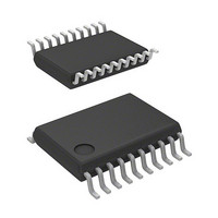
R5F21324CNSP#U0 Renesas Electronics America, R5F21324CNSP#U0 Datasheet - Page 466

R5F21324CNSP#U0
Manufacturer Part Number
R5F21324CNSP#U0
Description
MCU 1KB FLASH 16K ROM 20-LSSOP
Manufacturer
Renesas Electronics America
Series
R8C/3x/32Cr
Datasheet
1.R5F21321CDSPU0.pdf
(605 pages)
Specifications of R5F21324CNSP#U0
Core Processor
R8C
Core Size
16/32-Bit
Speed
20MHz
Connectivity
I²C, LIN, SIO, SSU, UART/USART
Peripherals
POR, PWM, Voltage Detect, WDT
Number Of I /o
15
Program Memory Size
16KB (16K x 8)
Program Memory Type
FLASH
Ram Size
1.5K x 8
Voltage - Supply (vcc/vdd)
1.8 V ~ 5.5 V
Data Converters
A/D 4x10b
Oscillator Type
Internal
Operating Temperature
-20°C ~ 85°C
Package / Case
20-LSSOP
Lead Free Status / RoHS Status
Lead free / RoHS Compliant
Eeprom Size
-
- Current page: 466 of 605
- Download datasheet (6Mb)
R8C/32C Group
REJ09B0573-0100 Rev.1.00 Dec. 18, 2009
Page 437 of 573
Figure 26.7
Hardware LIN Clear the status flags
Timer RA
Timer RA
Hardware LIN Set Synch Break detection to start
Hardware LIN Read the RXD0 input status flag
Hardware LIN Read the Synch Break detection flag
Set pulse width measurement to start
TSTART bit in TRACR register ← 1
Read the count status flag
TCSTF flag in TRACR register
Header Field Reception Flowchart Example (2)
RXDSF flag in LINCR register
SBDCT flag in LINST register
detection, Synch Field measurement)
Bits B2CLR, B1CLR, B0CLR in LINST
register ← 1
(Bus collision detection, Synch Break
LSTART bit in LINCR register ← 1
RXDSF = 1?
SBDCT = 1?
TCSTF = 1?
YES
YES
YES
A
B
NO
NO
NO
Wait until timer RA starts counting.
Zero or one cycle of the timer RA count
source is required after timer RA starts
counting before the TCSTF flag is set
to 1.
Wait until the RXD0 input to UART0 for
the hardware LIN is masked.
After writing 1 to the LSTART bit,
do not apply a “L” level to the RXD0 pin
until 1 is read from the RXDSF flag.
Otherwise, the signal applied during this
time will be input directly to UART0.
One or two cycles of the CPU clock and
zero or one cycle of the timer RA count
source are required after the LSTART bit
is set to 1 before the RXDSF flag is set
to 1. After this, input to timer RA and
UART0 is enabled.
A Synch Break for the hardware LIN is
detected.
A timer RA interrupt can be used.
When a Synch Break is detected, timer
RA is reloaded with the initially set count
value.
Even if the duration of the input “L” level
is shorter than the set period, timer RA is
reloaded with the initially set count value.
Wait until the next “L” level is input.
One or two cycles of the CPU clock are
required after Synch Break detection
before the SBDCT flag is
set to 1.
If the SBE bit in the LINCR register is set
to 0 (unmasked after Synch Break
detected), timer RA can be used in timer
mode after the SBDCT flag in the LINST
register is set to 1 and the RXDSF flag is
set to 0.
26. Hardware LIN
Related parts for R5F21324CNSP#U0
Image
Part Number
Description
Manufacturer
Datasheet
Request
R

Part Number:
Description:
KIT STARTER FOR M16C/29
Manufacturer:
Renesas Electronics America
Datasheet:

Part Number:
Description:
KIT STARTER FOR R8C/2D
Manufacturer:
Renesas Electronics America
Datasheet:

Part Number:
Description:
R0K33062P STARTER KIT
Manufacturer:
Renesas Electronics America
Datasheet:

Part Number:
Description:
KIT STARTER FOR R8C/23 E8A
Manufacturer:
Renesas Electronics America
Datasheet:

Part Number:
Description:
KIT STARTER FOR R8C/25
Manufacturer:
Renesas Electronics America
Datasheet:

Part Number:
Description:
KIT STARTER H8S2456 SHARPE DSPLY
Manufacturer:
Renesas Electronics America
Datasheet:

Part Number:
Description:
KIT STARTER FOR R8C38C
Manufacturer:
Renesas Electronics America
Datasheet:

Part Number:
Description:
KIT STARTER FOR R8C35C
Manufacturer:
Renesas Electronics America
Datasheet:

Part Number:
Description:
KIT STARTER FOR R8CL3AC+LCD APPS
Manufacturer:
Renesas Electronics America
Datasheet:

Part Number:
Description:
KIT STARTER FOR RX610
Manufacturer:
Renesas Electronics America
Datasheet:

Part Number:
Description:
KIT STARTER FOR R32C/118
Manufacturer:
Renesas Electronics America
Datasheet:

Part Number:
Description:
KIT DEV RSK-R8C/26-29
Manufacturer:
Renesas Electronics America
Datasheet:

Part Number:
Description:
KIT STARTER FOR SH7124
Manufacturer:
Renesas Electronics America
Datasheet:

Part Number:
Description:
KIT STARTER FOR H8SX/1622
Manufacturer:
Renesas Electronics America
Datasheet:

Part Number:
Description:
KIT DEV FOR SH7203
Manufacturer:
Renesas Electronics America
Datasheet:


