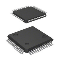
R5F21256SNFP#ES Renesas Electronics America, R5F21256SNFP#ES Datasheet - Page 505

R5F21256SNFP#ES
Manufacturer Part Number
R5F21256SNFP#ES
Description
MCU 2/5V 32K 52-LQFP ES SAMPLE
Manufacturer
Renesas Electronics America
Series
R8C/2x/25r
Specifications of R5F21256SNFP#ES
Core Processor
R8C
Core Size
16/32-Bit
Speed
20MHz
Connectivity
I²C, LIN, SIO, SSU, UART/USART
Peripherals
POR, Voltage Detect, WDT
Number Of I /o
41
Program Memory Size
32KB (32K x 8)
Program Memory Type
FLASH
Ram Size
2K x 8
Voltage - Supply (vcc/vdd)
2.2 V ~ 5.5 V
Data Converters
A/D 12x10b
Oscillator Type
Internal
Operating Temperature
-20°C ~ 85°C
Package / Case
52-LQFP
Lead Free Status / RoHS Status
Lead free / RoHS Compliant
Eeprom Size
-
Available stocks
Company
Part Number
Manufacturer
Quantity
Price
- Current page: 505 of 527
- Download datasheet (6Mb)
Rev.
0.10
0.20
REVISION HISTORY
REVISION HISTORY
Jan 16, 2006
Jul 27, 2005
Date
all pages • “Preliminary” deleted
Page
10
12
13
14
15
24
25
26
−
2
3
4
5
6
7
8
9
First Edition issued
• Symbol name “TRDMDR” → “TRDMR”, “SSUAIC” → “SSUIC”,
• Pin name “TCLK” → “TRDCLK” revised
• Bit name “TPSC0 to TPSC2” → “TCK0 to TCK2”, “TRD0 count stop bit”
Table 1.1 Functions and Specifications for R8C/24 Group revised
Table 1.2 Functions and Specifications for R8C/25 Group revised
Figure 1.1 Block Diagram;
Table 1.3 Product Information for R8C/24 Group revised
Table 1.4 Product Information of R8C/25 Group revised
Figure 1.4 Pin Assignment (Top View);
Table 1.5 Pin Functions;
Table 1.6 Pin Name Information by Pin Number
Figure 2.1 CPU Registers;
2.8.10 Reserved Area;
Figure 3.1 Memory Map of R8C/24 Group;
3.2 R8C/25 Group, Figure 3.2 Memory Map of R8C/25 Group;
Table 4.1 SFR Information(1);
Figure 5.4 OFS Register; NOTE1 revised and NOTE3 added
5.1.1 When Power Supply is Stable (2) revised
5.1.2 Power On (4) revised
Figure 5.5 Example of Hardware Reset Circuit and Operation and Figure
5.6 Example of Hardware Reset Circuit (Usage Example of External
Supply Voltage Detection Circuit) and Operation revised
“IIC2AIC” → “IICIC”, and “TSTOP0, TSTOP1” → “CSEL0, CSEL1”
revised
→ “TRD0 count operation select bit”, and “TRD1 count stop bit” →
“TRD1 count operation select bit” revised
R8C/24 Group, R8C/25 Group Hardware Manual
R8C/24 Group, R8C/25 Group Hardware Manual
“Peripheral Functions” added,
“System Clock Generation” → “System Clock Generator” revised
“VSS” → “VSS/AVSS” and “VCC” → “VCC/AVCC” revised
“Analog power supply input” added, “Reference voltage input” revised
“VSS” → “VSS/AVSS” and “VCC” → “VCC/AVCC” revised
“Reserved Area” → “Reserved Bit” revised
“Reserved Area” → “Reserved bit” revised
“Program area” → “program ROM” revised
“Data area” → “data flash”, “Program area” → “program ROM” revised
0012h:
0016h:
0024h:
NOTES 3 and 4 revised
“X0h” → “00h”
“X0h” → “00h”
“TBD” → “When shipping”
C - 1
Description
Summary
Related parts for R5F21256SNFP#ES
Image
Part Number
Description
Manufacturer
Datasheet
Request
R

Part Number:
Description:
KIT STARTER FOR M16C/29
Manufacturer:
Renesas Electronics America
Datasheet:

Part Number:
Description:
KIT STARTER FOR R8C/2D
Manufacturer:
Renesas Electronics America
Datasheet:

Part Number:
Description:
R0K33062P STARTER KIT
Manufacturer:
Renesas Electronics America
Datasheet:

Part Number:
Description:
KIT STARTER FOR R8C/23 E8A
Manufacturer:
Renesas Electronics America
Datasheet:

Part Number:
Description:
KIT STARTER FOR R8C/25
Manufacturer:
Renesas Electronics America
Datasheet:

Part Number:
Description:
KIT STARTER H8S2456 SHARPE DSPLY
Manufacturer:
Renesas Electronics America
Datasheet:

Part Number:
Description:
KIT STARTER FOR R8C38C
Manufacturer:
Renesas Electronics America
Datasheet:

Part Number:
Description:
KIT STARTER FOR R8C35C
Manufacturer:
Renesas Electronics America
Datasheet:

Part Number:
Description:
KIT STARTER FOR R8CL3AC+LCD APPS
Manufacturer:
Renesas Electronics America
Datasheet:

Part Number:
Description:
KIT STARTER FOR RX610
Manufacturer:
Renesas Electronics America
Datasheet:

Part Number:
Description:
KIT STARTER FOR R32C/118
Manufacturer:
Renesas Electronics America
Datasheet:

Part Number:
Description:
KIT DEV RSK-R8C/26-29
Manufacturer:
Renesas Electronics America
Datasheet:

Part Number:
Description:
KIT STARTER FOR SH7124
Manufacturer:
Renesas Electronics America
Datasheet:

Part Number:
Description:
KIT STARTER FOR H8SX/1622
Manufacturer:
Renesas Electronics America
Datasheet:

Part Number:
Description:
KIT DEV FOR SH7203
Manufacturer:
Renesas Electronics America
Datasheet:


