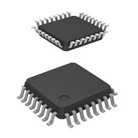
R5F212F4NFP#U0 Renesas Electronics America, R5F212F4NFP#U0 Datasheet - Page 13

R5F212F4NFP#U0
Manufacturer Part Number
R5F212F4NFP#U0
Description
MCU 1KB FLASH 16K ROM 32-LQFP
Manufacturer
Renesas Electronics America
Series
R8C/2x/2Fr
Datasheet
1.R5F212E2NFPU0.pdf
(43 pages)
Specifications of R5F212F4NFP#U0
Core Processor
R8C
Core Size
16/32-Bit
Speed
20MHz
Connectivity
LIN, SIO, UART/USART
Peripherals
POR, PWM, Voltage Detect, WDT
Number Of I /o
25
Program Memory Size
16KB (16K x 8)
Program Memory Type
FLASH
Ram Size
1K x 8
Voltage - Supply (vcc/vdd)
2.7 V ~ 5.5 V
Data Converters
A/D 12x10b; D/A 2x8b
Oscillator Type
Internal
Operating Temperature
-20°C ~ 85°C
Package / Case
32-LQFP
Lead Free Status / RoHS Status
Lead free / RoHS Compliant
Eeprom Size
-
Available stocks
Company
Part Number
Manufacturer
Quantity
Price
R8C/2E Group, R8C/2F Group
Rev.1.00
REJ03B0222-0100
1.5
Table 1.8
I: Input
NOTE:
Power supply input VCC, VSS
Analog power
supply input
Reset input
MODE
XIN clock input
XIN clock output
INT interrupt input
Key input interrupt
Timer RA
Timer RB
Timer RC
Timer RE
Serial interface
Reference voltage
input
A/D converter
D/A converter
Comparator
I/O port
Input port
Table 1.8 list Pin Functions.
1. Refer to the oscillator manufacturer for oscillation characteristics.
Type
Pin Functions
Dec 14, 2007
O: Output
Pin Functions
AVCC, AVSS
RESET
MODE
XIN
XOUT
INT0, INT1, INT3
KI0 to KI3
TRAO
TRAIO
TRBO
TRCCLK
TRCTRG
TRCIOA, TRCIOB,
TRCIOC, TRCIOD
TREO
CLK0
RXD0
TXD0
VREF
AN0 to AN11
DA0 to DA1
AVREF0 to AVREF1
ACMP0 to ACMP1
ACOUT0 to ACOUT1
P0_0 to P0_7,
P1_0 to P1_7,
P3_1, P3_3 to P3_7,
P4_5,
P5_3, P5_4
P4_2, P4_6, P4_7
Page 11 of 39
Symbol
I/O: Input and output
I/O Type
I/O
I/O
I/O
I/O
O
O
O
O
O
O
O
I
I
I
I
I
I
I
I
I
I
I
I
I
I
I
Apply 2.7 V to 5.5 V to the VCC pin. Apply 0 V to the VSS pin.
Power supply for the A/D converter.
Connect a capacitor between AVCC and AVSS.
Input “L” on this pin resets the MCU.
Connect this pin to VCC via a resistor.
Connect a ceramic resonator or a crystal oscillator between
the XIN and XOUT pins.
the XIN pin and leave the XOUT pin open.
INT interrupt input pins
Key input interrupt input pins
Timer RA output pin
Timer RA I/O pin
Timer RB output pin
External clock input pin
External trigger input pin
Sharing output-compare output / input-capture input / PWM /
PWM2 output pins
Timer RE output pin
Clock I/O pin
Receive data input pin
Transmit data output pin
Reference voltage input pin to A/D converter
Analog input pins to A/D converter
Reference voltage input pins to comparator
Analog voltage input pins to comparator
Comparison result output pins of comparator
CMOS I/O ports. Each port has an I/O select direction
register, allowing each pin in the port to be directed for input
or output individually.
Any port set to input can be set to use a pull-up resistor or not
by a program.
P1_0 to P1_7 also function as LED drive ports.
Input-only ports
These pins are provided for XIN clock generation circuit I/O.
Output pins from D/A converter
(1)
Description
To use an external clock, input it to
1. Overview


