R5F212F4NFP#U0 Renesas Electronics America, R5F212F4NFP#U0 Datasheet - Page 4
R5F212F4NFP#U0
Manufacturer Part Number
R5F212F4NFP#U0
Description
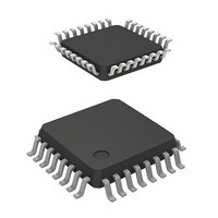
MCU 1KB FLASH 16K ROM 32-LQFP
Manufacturer
Renesas Electronics America
Series
R8C/2x/2Fr
Datasheet
1.R5F212E2NFPU0.pdf
(43 pages)
Specifications of R5F212F4NFP#U0
Core Processor
R8C
Core Size
16/32-Bit
Speed
20MHz
Connectivity
LIN, SIO, UART/USART
Peripherals
POR, PWM, Voltage Detect, WDT
Number Of I /o
25
Program Memory Size
16KB (16K x 8)
Program Memory Type
FLASH
Ram Size
1K x 8
Voltage - Supply (vcc/vdd)
2.7 V ~ 5.5 V
Data Converters
A/D 12x10b; D/A 2x8b
Oscillator Type
Internal
Operating Temperature
-20°C ~ 85°C
Package / Case
32-LQFP
Lead Free Status / RoHS Status
Lead free / RoHS Compliant
Eeprom Size
-
Available stocks
Company
Part Number
Manufacturer
Quantity
Price


R8C/2E Group, R8C/2F Group
Rev.1.00
REJ03B0222-0100
1.1.2
Table 1.1
CPU
Memory
Power Supply
Voltage
Detection
I/O Ports
Clock
Interrupts
Watchdog Timer
Timer
Serial
Interface
LIN Module
A/D Converter
D/A Converter
Comparator
Tables 1.1 and 1.2 outlines the Specifications for R8C/2E Group and Tables 1.3 and 1.4 outlines the
Specifications for R8C/2F Group.
Item
Dec 14, 2007
Specifications
Specifications for R8C/2E Group (1)
Central
ROM, RAM
processing unit
Voltage
detection circuit
Programmable
I/O ports
Clock generation
circuits
Timer RA
Timer RB
Timer RC
Timer RE
UART0
Function
Page 2 of 39
R8C/Tiny series core
• Number of fundamental instructions: 89
• Minimum instruction execution time:
• Multiplier: 16 bits × 16 bits → 32 bits
• Multiply-accumulate instruction: 16 bits × 16 bits + 32 bits → 32 bits
• Operation mode: Single-chip mode (address space: 1 Mbyte)
Refer to Table 1.5 Product List for R8C/2E Group.
• Power-on reset
• Voltage detection 2
• Input-only: 3 pins
• CMOS I/O ports: 25, selectable pull-up resistor
• High current drive ports: 8
2 circuits: XIN clock oscillation circuit (with on-chip feedback resistor),
• Oscillation stop detection: XIN clock oscillation stop detection
• Frequency divider circuit: Dividing selectable 1, 2, 4, 8, and 16
• Low power consumption modes:
• External: 4 sources, Internal: 13 sources, Software: 4 sources
• Priority levels: 7 levels
15 bits × 1 (with prescaler), reset start selectable
8 bits × 1 (with 8-bit prescaler)
8 bits × 1 (with 8-bit prescaler)
16 bits × 1 (with 4 capture/compare registers)
8 bits × 1
Clock synchronous serial I/O/UART × 1
Hardware LIN: 1 (timer RA, UART0)
10-bit resolution × 12 channels, includes sample and hold function
8-bit resolution × 2 circuits
2 circuits
Timer mode (period timer), pulse output mode (output level inverted
every period), event counter mode, pulse width measurement mode,
pulse period measurement mode
Timer mode (period timer), programmable waveform generation
mode (PWM output), programmable one-shot generation mode,
programmable wait one-shot generation mode
Timer mode (input capture function, output compare function), PWM
mode (output 3 pins), PWM2 mode (PWM output pin)
Output compare mode
Standard operating mode (high-speed clock, high-speed on-chip
oscillator, low-speed on-chip oscillator), wait mode, stop mode
50 ns (f(XIN) = 20 MHz, VCC = 3.0 to 5.5 V)
100 ns (f(XIN) = 10 MHz, VCC = 2.7 to 5.5 V)
On-chip oscillator (high-speed, low-speed)
(high-speed on-chip oscillator has a frequency adjustment
function)
function
Specification
1. Overview
Related parts for R5F212F4NFP#U0
Image
Part Number
Description
Manufacturer
Datasheet
Request
R

Part Number:
Description:
KIT STARTER FOR M16C/29
Manufacturer:
Renesas Electronics America
Datasheet:

Part Number:
Description:
KIT STARTER FOR R8C/2D
Manufacturer:
Renesas Electronics America
Datasheet:

Part Number:
Description:
R0K33062P STARTER KIT
Manufacturer:
Renesas Electronics America
Datasheet:

Part Number:
Description:
KIT STARTER FOR R8C/23 E8A
Manufacturer:
Renesas Electronics America
Datasheet:

Part Number:
Description:
KIT STARTER FOR R8C/25
Manufacturer:
Renesas Electronics America
Datasheet:

Part Number:
Description:
KIT STARTER H8S2456 SHARPE DSPLY
Manufacturer:
Renesas Electronics America
Datasheet:

Part Number:
Description:
KIT STARTER FOR R8C38C
Manufacturer:
Renesas Electronics America
Datasheet:

Part Number:
Description:
KIT STARTER FOR R8C35C
Manufacturer:
Renesas Electronics America
Datasheet:

Part Number:
Description:
KIT STARTER FOR R8CL3AC+LCD APPS
Manufacturer:
Renesas Electronics America
Datasheet:
Part Number:
Description:
KIT STARTER FOR RX610
Manufacturer:
Renesas Electronics America
Datasheet:

Part Number:
Description:
KIT STARTER FOR R32C/118
Manufacturer:
Renesas Electronics America
Datasheet:

Part Number:
Description:
KIT DEV RSK-R8C/26-29
Manufacturer:
Renesas Electronics America
Datasheet:

Part Number:
Description:
KIT STARTER FOR SH7124
Manufacturer:
Renesas Electronics America
Datasheet:

Part Number:
Description:
KIT STARTER FOR H8SX/1622
Manufacturer:
Renesas Electronics America
Datasheet:

Part Number:
Description:
KIT DEV FOR SH7203
Manufacturer:
Renesas Electronics America
Datasheet: