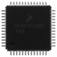
MC9S12C128CPBE Freescale Semiconductor, MC9S12C128CPBE Datasheet - Page 267

MC9S12C128CPBE
Manufacturer Part Number
MC9S12C128CPBE
Description
IC MCU 128K FLASH 25MHZ 52-LQFP
Manufacturer
Freescale Semiconductor
Series
HCS12r
Specifications of MC9S12C128CPBE
Core Processor
HCS12
Core Size
16-Bit
Speed
25MHz
Connectivity
CAN, EBI/EMI, SCI, SPI
Peripherals
POR, PWM, WDT
Number Of I /o
35
Program Memory Size
128KB (128K x 8)
Program Memory Type
FLASH
Ram Size
4K x 8
Voltage - Supply (vcc/vdd)
2.35 V ~ 5.5 V
Data Converters
A/D 8x10b
Oscillator Type
Internal
Operating Temperature
-40°C ~ 85°C
Package / Case
52-LQFP
Lead Free Status / RoHS Status
Lead free / RoHS Compliant
Eeprom Size
-
Available stocks
Company
Part Number
Manufacturer
Quantity
Price
Company:
Part Number:
MC9S12C128CPBE
Manufacturer:
Freescale Semiconductor
Quantity:
10 000
Company:
Part Number:
MC9S12C128CPBER
Manufacturer:
Freescale Semiconductor
Quantity:
10 000
- Current page: 267 of 690
- Download datasheet (4Mb)
The PLL is a frequency generator that operates in either acquisition mode or tracking mode, depending on
the difference between the output frequency and the target frequency. The PLL can change between
acquisition and tracking modes either automatically or manually.
The VCO has a minimum operating frequency, which corresponds to the self-clock mode frequency f
9.4.1.1
The oscillator output clock signal (OSCCLK) is fed through the reference programmable divider and is
divided in a range of 1 to 16 (REFDV+1) to output the reference clock. The VCO output clock, (PLLCLK)
is fed back through the programmable loop divider and is divided in a range of 2 to 128 in increments of
[2 x (SYNR +1)] to output the feedback clock. See
The phase detector then compares the feedback clock, with the reference clock. Correction pulses are
generated based on the phase difference between the two signals. The loop filter then slightly alters the DC
voltage on the external filter capacitor connected to XFC pin, based on the width and direction of the
correction pulse. The filter can make fast or slow corrections depending on its mode, as described in the
next subsection. The values of the external filter network and the reference frequency determine the speed
of the corrections and the stability of the PLL.
9.4.1.2
The lock detector compares the frequencies of the feedback clock, and the reference clock. Therefore, the
speed of the lock detector is directly proportional to the final reference frequency. The circuit determines
the mode of the PLL and the lock condition based on this comparison.
Freescale Semiconductor
EXTAL
XTAL
supplied by:
PLL Operation
Acquisition and Tracking Modes
VDDPLL/VSSPLL
VDD/VSS
CONSUMPTION
OSCILLATOR
REDUCED
OSCCLK
MONITOR
CRYSTAL
Figure 9-16. PLL Functional Diagram
MC9S12C-Family / MC9S12GC-Family
PROGRAMMABLE
REFDV <3:0>
REFERENCE
DIVIDER
PROGRAMMABLE
SYN <5:0>
DIVIDER
LOOP
Rev 01.24
Figure
REFERENCE
Chapter 9 Clocks and Reset Generator (CRGV4) Block Description
FEEDBACK
9-16.
DETECTOR
DETECTOR
FILTER
LOOP
PHASE
LOCK
PDET
VDDPLL
DOWN
UP
LOCK
CPUMP
XFC
PIN
VDDPLL/VSSPLL
VCO
PLLCLK
SCM
267
.
Related parts for MC9S12C128CPBE
Image
Part Number
Description
Manufacturer
Datasheet
Request
R
Part Number:
Description:
Manufacturer:
Freescale Semiconductor, Inc
Datasheet:
Part Number:
Description:
Manufacturer:
Freescale Semiconductor, Inc
Datasheet:
Part Number:
Description:
Manufacturer:
Freescale Semiconductor, Inc
Datasheet:
Part Number:
Description:
Manufacturer:
Freescale Semiconductor, Inc
Datasheet:
Part Number:
Description:
Manufacturer:
Freescale Semiconductor, Inc
Datasheet:
Part Number:
Description:
Manufacturer:
Freescale Semiconductor, Inc
Datasheet:
Part Number:
Description:
Manufacturer:
Freescale Semiconductor, Inc
Datasheet:
Part Number:
Description:
Manufacturer:
Freescale Semiconductor, Inc
Datasheet:
Part Number:
Description:
Manufacturer:
Freescale Semiconductor, Inc
Datasheet:
Part Number:
Description:
Manufacturer:
Freescale Semiconductor, Inc
Datasheet:
Part Number:
Description:
Manufacturer:
Freescale Semiconductor, Inc
Datasheet:
Part Number:
Description:
Manufacturer:
Freescale Semiconductor, Inc
Datasheet:
Part Number:
Description:
Manufacturer:
Freescale Semiconductor, Inc
Datasheet:
Part Number:
Description:
Manufacturer:
Freescale Semiconductor, Inc
Datasheet:
Part Number:
Description:
Manufacturer:
Freescale Semiconductor, Inc
Datasheet:


