HD64F2218UTF24 Renesas Electronics America, HD64F2218UTF24 Datasheet - Page 53
HD64F2218UTF24
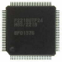
Manufacturer Part Number
HD64F2218UTF24
Description
IC H8S MCU FLASH 128K 100-TQFP
Manufacturer
Renesas Electronics America
Series
H8® H8S/2200r
Specifications of HD64F2218UTF24
Core Processor
H8S/2000
Core Size
16-Bit
Speed
24MHz
Connectivity
SCI, SmartCard, USB
Peripherals
DMA, POR, PWM, WDT
Number Of I /o
69
Program Memory Size
128KB (128K x 8)
Program Memory Type
FLASH
Ram Size
12K x 8
Voltage - Supply (vcc/vdd)
2.7 V ~ 3.6 V
Data Converters
A/D 6x10b
Oscillator Type
Internal
Operating Temperature
-20°C ~ 75°C
Package / Case
100-TQFP, 100-VQFP
For Use With
3DK2218-SS - KIT DEV H8S/2218 WINDOWS SIDESHW
Lead Free Status / RoHS Status
Contains lead / RoHS non-compliant
Eeprom Size
-
Available stocks
Company
Part Number
Manufacturer
Quantity
Price

Part Number:
HD64F2218UTF24V
Manufacturer:
RENESAS/瑞萨
Quantity:
20 000


Table 9.3
Table 9.4
Table 9.5
Table 9.6
Table 9.7
Table 9.8
Table 9.9
Table 9.10
Table 9.11
Table 9.12
Table 9.13
Table 9.14
Table 9.15
Table 9.16
Table 9.17
Table 9.18
Table 9.19
Table 9.20
Table 9.21
Table 9.22
Table 9.23
Table 9.24
Section 10 Watchdog Timer (WDT)
Table 10.1
Section 11 Realtime Clock (RTC)
Table 11.1
Table 11.2
Table 11.3
Section 12 Serial Communication Interface
Table 12.1
Table 12.2
Table 12.3
Table 12.4
Table 12.5
Table 12.6
Table 12.7
Table 12.8
CCLR2 to CCLR0 (channel 0) ............................................................................... 280
CCLR2 to CCLR0 (channels 1 and 2).................................................................... 280
TPSC2 to TPSC0 (channel 0)................................................................................. 281
TPSC2 to TPSC0 (channel 1)................................................................................. 281
TPSC2 to TPSC0 (channel 2)................................................................................. 282
MD3 to MD0.......................................................................................................... 283
TIORH_0 (channel 0)............................................................................................. 285
TIORH_0 (channel 0)............................................................................................. 286
TIORL_0 (channel 0) ............................................................................................. 287
TIORL_0 (channel 0) ............................................................................................. 288
TIOR_1 (channel 1)................................................................................................ 289
TIOR_1 (channel 1)................................................................................................ 290
TIOR_2 (channel 2)................................................................................................ 291
TIOR_2 (channel 2)................................................................................................ 292
Register Combinations in Buffer Operation........................................................... 309
PWM Output Registers and Output Pins................................................................ 314
Phase Counting Mode Clock Input Pins................................................................. 317
Up/Down-Count Conditions in Phase Counting Mode 1 ....................................... 318
Up/Down-Count Conditions in Phase Counting Mode 2 ....................................... 319
Up/Down-Count Conditions in Phase Counting Mode 3 ....................................... 320
Up/Down-Count Conditions in Phase Counting Mode 4 ....................................... 321
TPU Interrupts........................................................................................................ 322
WDT Interrupt Source............................................................................................ 345
Pin Configuration ................................................................................................... 350
Interrupt Source...................................................................................................... 360
Operating State in Each Mode................................................................................ 362
Pin Configuration ................................................................................................... 367
Relationships between the N Setting in BRR and Bit Rate B ................................ 395
BRR Settings for Various Bit Rates (Asynchronous Mode) .................................. 396
Maximum Bit Rate for Each Frequency (Asynchronous Mode) ............................ 399
Maximum Bit Rate with External Clock Input (Asynchronous Mode) .................. 400
BRR Settings for Various Bit Rates (Clocked Synchronous Mode) ...................... 401
Maximum Bit Rate with External Clock Input (Clocked Synchronous Mode) ...... 401
BRR Settings for Various Bit Rates
(Smart Card Interface Mode, when n = 0 and S = 372).......................................... 402
Rev.7.00 Dec. 24, 2008 Page li of liv
REJ09B0074-0700
Related parts for HD64F2218UTF24
Image
Part Number
Description
Manufacturer
Datasheet
Request
R

Part Number:
Description:
KIT STARTER FOR M16C/29
Manufacturer:
Renesas Electronics America
Datasheet:

Part Number:
Description:
KIT STARTER FOR R8C/2D
Manufacturer:
Renesas Electronics America
Datasheet:

Part Number:
Description:
R0K33062P STARTER KIT
Manufacturer:
Renesas Electronics America
Datasheet:

Part Number:
Description:
KIT STARTER FOR R8C/23 E8A
Manufacturer:
Renesas Electronics America
Datasheet:

Part Number:
Description:
KIT STARTER FOR R8C/25
Manufacturer:
Renesas Electronics America
Datasheet:

Part Number:
Description:
KIT STARTER H8S2456 SHARPE DSPLY
Manufacturer:
Renesas Electronics America
Datasheet:

Part Number:
Description:
KIT STARTER FOR R8C38C
Manufacturer:
Renesas Electronics America
Datasheet:

Part Number:
Description:
KIT STARTER FOR R8C35C
Manufacturer:
Renesas Electronics America
Datasheet:

Part Number:
Description:
KIT STARTER FOR R8CL3AC+LCD APPS
Manufacturer:
Renesas Electronics America
Datasheet:
Part Number:
Description:
KIT STARTER FOR RX610
Manufacturer:
Renesas Electronics America
Datasheet:

Part Number:
Description:
KIT STARTER FOR R32C/118
Manufacturer:
Renesas Electronics America
Datasheet:

Part Number:
Description:
KIT DEV RSK-R8C/26-29
Manufacturer:
Renesas Electronics America
Datasheet:

Part Number:
Description:
KIT STARTER FOR SH7124
Manufacturer:
Renesas Electronics America
Datasheet:

Part Number:
Description:
KIT STARTER FOR H8SX/1622
Manufacturer:
Renesas Electronics America
Datasheet:

Part Number:
Description:
KIT DEV FOR SH7203
Manufacturer:
Renesas Electronics America
Datasheet: