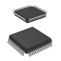
DF36034HJ Renesas Electronics America, DF36034HJ Datasheet - Page 195

DF36034HJ
Manufacturer Part Number
DF36034HJ
Description
MCU 3/5V 32K J-TEMP 64=QFP
Manufacturer
Renesas Electronics America
Series
H8® H8/300H Tinyr
Datasheet
1.DF36057GFZV.pdf
(594 pages)
Specifications of DF36034HJ
Core Processor
H8/300H
Core Size
16-Bit
Speed
20MHz
Connectivity
CAN, SCI, SSU
Peripherals
PWM, WDT
Number Of I /o
45
Program Memory Size
32KB (32K x 8)
Program Memory Type
FLASH
Ram Size
2K x 8
Voltage - Supply (vcc/vdd)
3 V ~ 5.5 V
Data Converters
A/D 8x10b
Oscillator Type
Internal
Operating Temperature
-40°C ~ 85°C
Package / Case
64-QFP
Lead Free Status / RoHS Status
Contains lead / RoHS non-compliant
Eeprom Size
-
Other names
HD64F36034HJ
HD64F36034HJ
HD64F36034HJ
- Current page: 195 of 594
- Download datasheet (4Mb)
11.6
The following types of contention or operation can occur in timer V operation.
1. Writing to registers is performed in the T3 state of a TCNTV write cycle. If a TCNTV clear
2. If a compare match is generated in the T3 state of a TCORA or TCORB write cycle, the write
3. If compare matches A and B occur simultaneously, any conflict between the output selections
4. Depending on the timing, TCNTV may be incremented by a switch between different internal
signal is generated in the T3 state of a TCNTV write cycle, as shown in figure 11.11, clearing
takes precedence and the write to the counter is not carried out. If counting-up is generated in
the T3 state of a TCNTV write cycle, writing takes precedence.
to TCORA or TCORB takes precedence and the compare match signal is inhibited. Figure
11.12 shows the timing.
for compare match A and compare match B is resolved by the following priority: toggle output
clock sources. When TCNTV is internally clocked, an increment pulse is generated from the
falling edge of an internal clock signal that is a divided system clock ( ). Therefore, as shown
in figure 11.3 the switch is from a high clock signal to a low clock signal, the switchover is
seen as a falling edge, causing TCNTV to increment. TCNTV can also be incremented by a
switch between internal and external clocks.
output 1 output 0.
Usage Notes
Figure 11.11 Contention between TCNTV Write and Clear
Counter clear signal
Internal write signal
Address
TCNTV
TCNTV write cycle by CPU
T
1
TCNTV address
N
T
2
Rev. 4.00 Mar. 15, 2006 Page 161 of 556
T
3
H'00
Section 11 Timer V
REJ09B0026-0400
Related parts for DF36034HJ
Image
Part Number
Description
Manufacturer
Datasheet
Request
R

Part Number:
Description:
KIT STARTER FOR M16C/29
Manufacturer:
Renesas Electronics America
Datasheet:

Part Number:
Description:
KIT STARTER FOR R8C/2D
Manufacturer:
Renesas Electronics America
Datasheet:

Part Number:
Description:
R0K33062P STARTER KIT
Manufacturer:
Renesas Electronics America
Datasheet:

Part Number:
Description:
KIT STARTER FOR R8C/23 E8A
Manufacturer:
Renesas Electronics America
Datasheet:

Part Number:
Description:
KIT STARTER FOR R8C/25
Manufacturer:
Renesas Electronics America
Datasheet:

Part Number:
Description:
KIT STARTER H8S2456 SHARPE DSPLY
Manufacturer:
Renesas Electronics America
Datasheet:

Part Number:
Description:
KIT STARTER FOR R8C38C
Manufacturer:
Renesas Electronics America
Datasheet:

Part Number:
Description:
KIT STARTER FOR R8C35C
Manufacturer:
Renesas Electronics America
Datasheet:

Part Number:
Description:
KIT STARTER FOR R8CL3AC+LCD APPS
Manufacturer:
Renesas Electronics America
Datasheet:

Part Number:
Description:
KIT STARTER FOR RX610
Manufacturer:
Renesas Electronics America
Datasheet:

Part Number:
Description:
KIT STARTER FOR R32C/118
Manufacturer:
Renesas Electronics America
Datasheet:

Part Number:
Description:
KIT DEV RSK-R8C/26-29
Manufacturer:
Renesas Electronics America
Datasheet:

Part Number:
Description:
KIT STARTER FOR SH7124
Manufacturer:
Renesas Electronics America
Datasheet:

Part Number:
Description:
KIT STARTER FOR H8SX/1622
Manufacturer:
Renesas Electronics America
Datasheet:

Part Number:
Description:
KIT DEV FOR SH7203
Manufacturer:
Renesas Electronics America
Datasheet:


