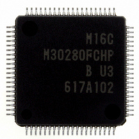
M30280FCHP#U3B Renesas Electronics America, M30280FCHP#U3B Datasheet - Page 417

M30280FCHP#U3B
Manufacturer Part Number
M30280FCHP#U3B
Description
IC M16C/28 MCU FLASH 128K 80LQFP
Manufacturer
Renesas Electronics America
Series
M16C™ M16C/Tiny/28r
Datasheet
1.M30280F6HPU9.pdf
(425 pages)
Specifications of M30280FCHP#U3B
Core Processor
M16C/60
Core Size
16-Bit
Speed
20MHz
Connectivity
I²C, IEBus, SIO, UART/USART
Peripherals
DMA, POR, PWM, Voltage Detect, WDT
Number Of I /o
71
Program Memory Size
128KB (128K x 8)
Program Memory Type
FLASH
Ram Size
12K x 8
Voltage - Supply (vcc/vdd)
2.7 V ~ 5.5 V
Data Converters
A/D 24x10b
Oscillator Type
Internal
Operating Temperature
-40°C ~ 85°C
Package / Case
80-LQFP
For Use With
R0K330290S000BE - KIT EVAL STARTER FOR M16C/29M30290T2-CPE - EMULATOR COMPACT M16C/26A/28/29M30290T2-CPE-HP - EMULATOR COMPACT FOR M16C/TINY
Lead Free Status / RoHS Status
Lead free / RoHS Compliant
Eeprom Size
-
Available stocks
Company
Part Number
Manufacturer
Quantity
Price
Part Number:
M30280FCHP#U3BM30280FCHP#U5B
Manufacturer:
Renesas Electronics America
Quantity:
135
Part Number:
M30280FCHP#U3BM30280FCHP#U5B
Manufacturer:
Renesas Electronics America
Quantity:
10 000
Part Number:
M30280FCHP#U3BM30280FCHP#U7B
Manufacturer:
Renesas Electronics America
Quantity:
10 000
- Current page: 417 of 425
- Download datasheet (4Mb)
Rev.
REVISION HISTORY
Date
Page
10
11
19
24
25
27
35
37
45
45
47
49
50
58
59
63
65
84
85
86
7
8
9
-
• Figure 1.3 Produt Numbering System is modified
• Table 1.4 Product Code None-lead free packages are deleted
• Table 1.5 Product Code - 85-pin Devise is added with note 1
• Figure 1.4 Marking Diagram is modified
• Figure 1.5 Pin Assignment of 85-pin Package is added
• Table 1.6 to 1.8 Pin Characteristics for 85-, 80-, and 64-pin Packages are
• Table 1.9 Pin Description Tables are modified
Memory
• Figure 3.1 Memory Map Internal RAM and ROM areas are modified
Special Function Register
• Table 4.1 SFR Information(1) Note 3 is deleted
• Table 4.3 SFR Information(3) LPCC0 and LPCC1 registers are added, value
Reset
• Figure 5.4 Voltage Detection Circuit Block modified
• Figure 5.7 Typical Operation of Voltage Down Detection Reset VC26 and
Clock Generation Circuit
• Figure 7.1 Clock Generation Circuit Upper portion of figure is modified
• Figure 7.4 ROCR Register Value after reset and reserved bit map are modified
• Figure 7.6 PCLKR Register and PM2 Register Note 2 is modified
• Figure 7.8 Examples of Main Clock Connection Circuit is modified
• Figure 7.9 Examples of Sub Clock Connection Circuit is modified
• Figure 7.11 State Transition to Stop Mode and Wait Mode Note 7 is added
• Figure 7.12 State Transition in Normal Mode Note 5 is simplified
• Figure 7.13 Switching Procedure from On-chip Oscillator Clock to Main
Interrupt
• Note is modified
Watchdog Timer
• Additional information of the WDTS register is inserted
• Figure 10.2 WDC Register and WDTS Register Note 1 of WDTS register is
• 10.2 Cold Start/Warm Start Information is all deleted
DMAC
• Note is modified
added
after reset of ROCR register is modified
VC27 bit lines are modified
between low-speed mode and low power dissipation mode
Clock is modified
deleted
M16C/28 Group (M16C/28, M16C/28B) Hardware Manual
C-10
Description
Summary
Related parts for M30280FCHP#U3B
Image
Part Number
Description
Manufacturer
Datasheet
Request
R

Part Number:
Description:
KIT STARTER FOR M16C/29
Manufacturer:
Renesas Electronics America
Datasheet:

Part Number:
Description:
KIT STARTER FOR R8C/2D
Manufacturer:
Renesas Electronics America
Datasheet:

Part Number:
Description:
R0K33062P STARTER KIT
Manufacturer:
Renesas Electronics America
Datasheet:

Part Number:
Description:
KIT STARTER FOR R8C/23 E8A
Manufacturer:
Renesas Electronics America
Datasheet:

Part Number:
Description:
KIT STARTER FOR R8C/25
Manufacturer:
Renesas Electronics America
Datasheet:

Part Number:
Description:
KIT STARTER H8S2456 SHARPE DSPLY
Manufacturer:
Renesas Electronics America
Datasheet:

Part Number:
Description:
KIT STARTER FOR R8C38C
Manufacturer:
Renesas Electronics America
Datasheet:

Part Number:
Description:
KIT STARTER FOR R8C35C
Manufacturer:
Renesas Electronics America
Datasheet:

Part Number:
Description:
KIT STARTER FOR R8CL3AC+LCD APPS
Manufacturer:
Renesas Electronics America
Datasheet:

Part Number:
Description:
KIT STARTER FOR RX610
Manufacturer:
Renesas Electronics America
Datasheet:

Part Number:
Description:
KIT STARTER FOR R32C/118
Manufacturer:
Renesas Electronics America
Datasheet:

Part Number:
Description:
KIT DEV RSK-R8C/26-29
Manufacturer:
Renesas Electronics America
Datasheet:

Part Number:
Description:
KIT STARTER FOR SH7124
Manufacturer:
Renesas Electronics America
Datasheet:

Part Number:
Description:
KIT STARTER FOR H8SX/1622
Manufacturer:
Renesas Electronics America
Datasheet:

Part Number:
Description:
KIT DEV FOR SH7203
Manufacturer:
Renesas Electronics America
Datasheet:


