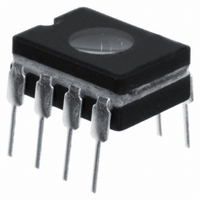
PIC12C672/JW Microchip Technology, PIC12C672/JW Datasheet - Page 406

PIC12C672/JW
Manufacturer Part Number
PIC12C672/JW
Description
IC MCU EPROM 2KX14 A/D 8CDIP
Manufacturer
Microchip Technology
Series
PIC® 12Cr
Datasheets
1.PIC16F688T-ISL.pdf
(688 pages)
2.PIC12CE673-10P.pdf
(129 pages)
3.PIC12CE673-10P.pdf
(14 pages)
Specifications of PIC12C672/JW
Core Processor
PIC
Core Size
8-Bit
Speed
10MHz
Peripherals
POR, WDT
Number Of I /o
5
Program Memory Size
3.5KB (2K x 14)
Program Memory Type
EPROM, UV
Ram Size
128 x 8
Voltage - Supply (vcc/vdd)
3 V ~ 5.5 V
Data Converters
A/D 4x8b
Oscillator Type
Internal
Operating Temperature
0°C ~ 70°C
Package / Case
8-CDIP (0.300", 7.62mm) Window
Lead Free Status / RoHS Status
Contains lead / RoHS non-compliant
Eeprom Size
-
Connectivity
-
Other names
Q395827
Available stocks
Company
Part Number
Manufacturer
Quantity
Price
Company:
Part Number:
PIC12C672/JW
Manufacturer:
MICKO
Quantity:
2 100
- Current page: 406 of 688
- Download datasheet (3Mb)
PICmicro MID-RANGE MCU FAMILY
Register 22-2:
DS31022A-page 22-4
bit 7:2
bit 1:0
bit 2:0
ADCON1 Register
bit 7
Unimplemented: Read as '0'
PCFG1:PCFG0: A/D Port Configuration Control bits
PCFG2:PCFG0: A/D Port Configuration Control bits
Legend
R = Readable bit
U = Unimplemented bit, read as ‘0’
Note 1: Some devices add an additional Port configuration bit (PCFG2). This allows the min-
Note 2: On any device reset, the Port pins multiplexed with analog functions (ANx) are
Note:
U-0
A = Analog input
D = Digital I/O
A = Analog input
D = Digital I/O
—
Note:
Note:
PCFG1:PCFG0
PCFG2:PCFG0
000
001
010
011
100
101
110
111
imum number of analog channels to be one. This is of most benefit to the 8-pin
devices with the A/D converter, since in an 8-pin device I/O is a premium resource.
In the other devices this bit is unimplemented, and read as ‘0’.
forced to be an analog input.
Some devices implement bit2 as the PCFG2 bit.
00
01
10
11
U-0
—
When AN3 is selected as V
pin. When AN3 is selected as an analog input (A), then the voltage reference for
the A/D is the device V
When AN1 is selected as V
pin. When AN1 is selected as an analog input (A), then the voltage reference for
the A/D is the device V
W = Writable bit
U-0
—
V
AN3
AN3
REF
A
D
D
A
A
D
D
D
D
D
D
+
U-0
—
DD
DD
AN2
AN2
.
.
A
A
D
D
A
A
A
A
D
D
D
D
- n = Value at POR reset
REF
REF
U-0
—
+, the A/D reference is the voltage on the AN3
+, the A/D reference is the voltage on the AN1
V
V
V
— / PCFG2
AN1
AN1
REF
REF
REF
U-0 / R/W-0
D
D
D
A
A
A
A
A
A
(1)
+
+
+
AN0
AN0
(1)
D
D
A
A
A
A
A
A
A
A
A
A
1997 Microchip Technology Inc.
PCFG1
R/W-0
bit 0
PCFG0
R/W-0
Related parts for PIC12C672/JW
Image
Part Number
Description
Manufacturer
Datasheet
Request
R

Part Number:
Description:
8-Pin/ 8-Bit CMOS Microcontroller with EEPROM Data Memory
Manufacturer:
Microchip Technology

Part Number:
Description:
IC, 8BIT MCU, PIC12, 32MHZ, DFN-8
Manufacturer:
Microchip Technology
Datasheet:

Part Number:
Description:
IC, 8BIT MCU, PIC12, 32MHZ, DFN-8
Manufacturer:
Microchip Technology
Datasheet:

Part Number:
Description:
Manufacturer:
Microchip Technology Inc.
Datasheet:

Part Number:
Description:
Manufacturer:
Microchip Technology Inc.
Datasheet:

Part Number:
Description:
Manufacturer:
Microchip Technology Inc.
Datasheet:

Part Number:
Description:
Manufacturer:
Microchip Technology Inc.
Datasheet:

Part Number:
Description:
Manufacturer:
Microchip Technology Inc.
Datasheet:

Part Number:
Description:
Manufacturer:
Microchip Technology Inc.
Datasheet:

Part Number:
Description:
Manufacturer:
Microchip Technology Inc.
Datasheet:


