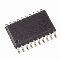
AT90S1200-4SC Atmel, AT90S1200-4SC Datasheet - Page 45

AT90S1200-4SC
Manufacturer Part Number
AT90S1200-4SC
Description
MCU 1K ISP FLASH 4MHZ 20-SOIC
Manufacturer
Atmel
Series
AVR® 90Sr
Datasheet
1.AT90S1200-12PC.pdf
(71 pages)
Specifications of AT90S1200-4SC
Core Processor
AVR
Core Size
8-Bit
Speed
4MHz
Connectivity
SPI
Peripherals
POR, WDT
Number Of I /o
15
Program Memory Size
1KB (512 x 16)
Program Memory Type
FLASH
Eeprom Size
64 x 8
Voltage - Supply (vcc/vdd)
2.7 V ~ 6 V
Oscillator Type
Internal
Operating Temperature
0°C ~ 70°C
Package / Case
20-SOIC (7.5mm Width)
Lead Free Status / RoHS Status
Contains lead / RoHS non-compliant
Ram Size
-
Data Converters
-
Available stocks
Company
Part Number
Manufacturer
Quantity
Price
Part Number:
AT90S1200-4SC
Manufacturer:
ATMEL/爱特梅尔
Quantity:
20 000
Data Polling EEPROM
Data Polling Flash
0838H–AVR–03/02
3. If a Chip Erase is performed (must be done to erase the Flash), wait t
4. The Flash or EEPROM array is programmed one byte at a time by supplying the
5. Any memory location can be verified by using the Read instruction which returns
6. Power-off sequence (if needed):
When a byte is being programmed into the EEPROM, reading the address location
being programmed will give the value P1 until the auto-erase is finished, and then the
value P2. See Table 18 for P1 and P2 values.
At the time the device is ready for a new EEPROM byte, the programmed value will read
correctly. This is used to determine when the next byte can be written. This will not work
for the values P1 and P2, so when programming these values, the user will have to wait
for at least the prescribed time
for
addresses that are meant to contain $FF can be skipped. This does not apply if the
EEPROM is reprogrammed without first chip-erasing the device.
Table 18. Read Back Value during EEPROM Polling
When a byte is being programmed into the Flash, reading the address location being
programmed will give the value $FF. At the time the device is ready for a new byte, the
programmed value will read correctly. This is used to determine when the next byte can
be written. This will not work for the value $FF, so when programming this value, the
user will have to wait for at least t
erased device contains $FF in all locations, programming of addresses that are meant
to contain $FF, can be skipped.
Part
AT90S1200
t
WD_PROG
At the end of the programming session, RESET can be set high to commence nor-
mal operation.
Set XTAL1 to “0” (if a crystal is not used or the device is running from the Internal
RC Oscillator).
Set RESET to “1”.
Turn V
after the instruction, give RESET a positive pulse, and start over from step 2.
See Table 21 on page 47 for t
address and data together with the appropriate Write instruction. An EEPROM
memory location is first automatically erased before new data is written. Wait
t
data file(s) needs to be programmed. See Table 22 on page 47 for t
value.
the content at the selected address at the serial output MISO (PB6) pin.
WD_PROG
CC
value. As a chip-erased device contains $FF in all locations, programming of
after transmitting the instruction. In an erased device, no $FFs in the
power off.
t
WD_PROG
WD_PROG
WD_ERASE
before programming the next byte. See Table 22
before programming the next byte. As a chip-
value.
P1
$00
AT90S1200
P2
$FF
WD_PROG
WD_ERASE
45


