ATMEGA163-8AI Atmel, ATMEGA163-8AI Datasheet - Page 155
ATMEGA163-8AI
Manufacturer Part Number
ATMEGA163-8AI
Description
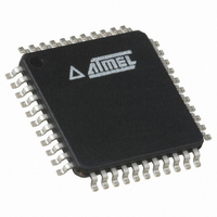
IC AVR MCU 16K A/D 8MHZ 44TQFP
Manufacturer
Atmel
Series
AVR® ATmegar
Datasheet
1.ATMEGA163-8AC.pdf
(187 pages)
Specifications of ATMEGA163-8AI
Core Processor
AVR
Core Size
8-Bit
Speed
8MHz
Connectivity
I²C, SPI, UART/USART
Peripherals
Brown-out Detect/Reset, POR, PWM, WDT
Number Of I /o
32
Program Memory Size
16KB (8K x 16)
Program Memory Type
FLASH
Eeprom Size
512 x 8
Ram Size
1K x 8
Voltage - Supply (vcc/vdd)
4 V ~ 5.5 V
Data Converters
A/D 8x10b
Oscillator Type
Internal
Operating Temperature
-40°C ~ 85°C
Package / Case
44-TQFP, 44-VQFP
Lead Free Status / RoHS Status
Contains lead / RoHS non-compliant
Available stocks
Company
Part Number
Manufacturer
Quantity
Price

Part Number:
ATMEGA163-8AI
Manufacturer:
ATMEL/爱特梅尔
Quantity:
20 000


Serial Programming
Algorithm
1142E–AVR–02/03
When writing serial data to the ATmega163, data is clocked on the rising edge of SCK.
When reading data from the ATmega163, data is clocked on the falling edge of SCK.
See Figure 87, Figure 88 and Table 62 for timing details.
To program and verify the ATmega163 in the serial programming mode, the following
sequence is recommended (See four byte instruction formats in Table 61):
1. Power-up sequence:
2. Wait for at least 20 ms and enable serial programming by sending the Program-
3. The Serial Programming instructions will not work if the communication is out of
4. If a Chip Erase is performed (must be done to erase the Flash), wait 2•t
5. The Flash is programmed one page at a time. The memory page is loaded one
6. The EEPROM array is programmed one byte at a time by supplying the address
7. Any memory location can be verified by using the Read instruction which returns
8. At the end of the programming session, RESET can be set high to commence
9. Power-off sequence (if needed):
Apply power between V
dance with the setting of CKSEL Fuses, apply a crystal/resonator, external clock, or
RC network, or let the device run on the internal RC Oscillator. In some systems,
the programmer can not guarantee that SCK is held low during power-up. In this
case, wait for 100 ms after SCK has been set to “0”. RESET must be then given a
positive pulse of at least two XTAL1 cycles duration and then set to “0”.
ming Enable serial instruction to pin MOSI/PB5.
synchronization. When in sync. the second byte ($53), will echo back when issu-
ing the third byte of the Programming Enable instruction. Whether the echo is
correct or not, all four bytes of the instruction must be transmitted. If the $53 did
not echo back, give SCK a positive pulse and issue a new Programming Enable
command. If the $53 is not seen within 32 attempts, there is no functional device
connected.
after the instruction, give RESET a positive pulse, and start over from Step 2.
See Table 60 for the t
byte at a time by supplying the 6 LSB of the address and data together with the
Load Program Memory Page instruction. The Program Memory Page is stored
by loading the Write Program Memory Page instruction with the 7 MSB of the
address. If polling is not used, the user must wait at least t
ing the next page. (Please refer to Table 60). Accessing the serial programming
interface before the Flash write operation completes can result in incorrect
programming.
and data together with the appropriate Write instruction. An EEPROM memory
location is first automatically erased before new data is written. If polling is not
used, the user must wait at least t
refer to Table 60). In a chip erased device, no $FFs in the data file(s) need to be
programmed.
the content at the selected address at serial output MISO/PB6.
normal operation.
Set XTAL1 to “0” (if external clock is used).
Set RESET to “1”.
Turn V
CC
power-off.
WD_FLASH
CC
and GND while RESET and SCK are set to “0”. In accor-
figure.
WD_EEPROM
before issuing the next byte. (Please
ATmega163(L)
WD_FLASH
before issu-
WD_FLASH
155
Related parts for ATMEGA163-8AI
Image
Part Number
Description
Manufacturer
Datasheet
Request
R

Part Number:
Description:
Manufacturer:
Atmel Corporation
Datasheet:

Part Number:
Description:
IC AVR MCU 16K 16MHZ 5V 44TQFP
Manufacturer:
Atmel
Datasheet:

Part Number:
Description:
IC AVR MCU 16K 16MHZ 5V 44-QFN
Manufacturer:
Atmel
Datasheet:

Part Number:
Description:
IC AVR MCU 16K 16MHZ 5V 40DIP
Manufacturer:
Atmel
Datasheet:
Part Number:
Description:
MCU AVR 16K FLASH 16MHZ 44-QFN
Manufacturer:
Atmel
Datasheet:
Part Number:
Description:
IC AVR MCU 16K 16MHZ COM 40-DIP
Manufacturer:
Atmel
Datasheet:
Part Number:
Description:
IC AVR MCU 16K 16MHZ COM 44-QFN
Manufacturer:
Atmel
Datasheet:
Part Number:
Description:
IC AVR MCU 16K 16MHZ IND 40-DIP
Manufacturer:
Atmel
Datasheet:
Part Number:
Description:
IC AVR MCU 16K 16MHZ IND 44-QFN
Manufacturer:
Atmel
Datasheet:
Part Number:
Description:
IC AVR MCU 16K 16MHZ IND 44-TQFP
Manufacturer:
Atmel
Datasheet:
Part Number:
Description:
IC MCU 8BIT 16KB FLASH 44TQFP
Manufacturer:
Atmel
Datasheet:
Part Number:
Description:
MCU AVR 16K FLASH 16MHZ 44-TQFP
Manufacturer:
Atmel
Datasheet:
Part Number:
Description:
IC AVR MCU 16K 16MHZ COM 44-TQFP
Manufacturer:
Atmel
Datasheet: