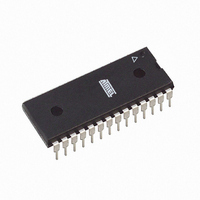
ATMEGA8L-8PC Atmel, ATMEGA8L-8PC Datasheet - Page 105

ATMEGA8L-8PC
Manufacturer Part Number
ATMEGA8L-8PC
Description
IC AVR MCU 8K LV 8MHZ COM 28-DIP
Manufacturer
Atmel
Series
AVR® ATmegar
Specifications of ATMEGA8L-8PC
Core Processor
AVR
Core Size
8-Bit
Speed
8MHz
Connectivity
I²C, SPI, UART/USART
Peripherals
Brown-out Detect/Reset, POR, PWM, WDT
Number Of I /o
23
Program Memory Size
8KB (4K x 16)
Program Memory Type
FLASH
Eeprom Size
512 x 8
Ram Size
1K x 8
Voltage - Supply (vcc/vdd)
2.7 V ~ 5.5 V
Data Converters
A/D 6x10b
Oscillator Type
Internal
Operating Temperature
0°C ~ 70°C
Package / Case
28-DIP (0.300", 7.62mm)
Lead Free Status / RoHS Status
Contains lead / RoHS non-compliant
Other names
ATMEGA8L8PC
Available stocks
Company
Part Number
Manufacturer
Quantity
Price
Company:
Part Number:
ATMEGA8L-8PC
Manufacturer:
TI
Quantity:
2 154
- Current page: 105 of 302
- Download datasheet (6Mb)
Output Compare
Unit
2486Z–AVR–02/11
The 8-bit comparator continuously compares TCNT2 with the Output Compare Register
(OCR2). Whenever TCNT2 equals OCR2, the comparator signals a match. A match will set the
Output Compare Flag (OCF2) at the next timer clock cycle. If enabled (OCIE2 = 1), the Output
Compare Flag generates an Output Compare interrupt. The OCF2 Flag is automatically cleared
when the interrupt is executed. Alternatively, the OCF2 Flag can be cleared by software by writ-
ing a logical one to its I/O bit location. The waveform generator uses the match signal to
generate an output according to operating mode set by the WGM21:0 bits and Compare Output
mode (COM21:0) bits. The max and bottom signals are used by the waveform generator for han-
dling the special cases of the extreme values in some modes of operation (see
Operation” on page
Figure 47
Figure 47. Output Compare Unit, Block Diagram
The OCR2 Register is double buffered when using any of the Pulse Width Modulation (PWM)
modes. For the normal and Clear Timer on Compare (CTC) modes of operation, the double buff-
ering is disabled. The double buffering synchronizes the update of the OCR2 Compare Register
to either top or bottom of the counting sequence. The synchronization prevents the occurrence
of odd-length, non-symmetrical PWM pulses, thereby making the output glitch-free.
The OCR2 Register access may seem complex, but this is not case. When the double buffering
is enabled, the CPU has access to the OCR2 Buffer Register, and if double buffering is disabled
the CPU will access the OCR2 directly.
shows a block diagram of the Output Compare unit.
BOTTOM
FOCn
TOP
108).
OCRn
Waveform Generator
WGMn1:0
=
(8-bit Comparator )
DATA BUS
COMn1:0
TCNTn
OCFn (Int. Req.)
ATmega8(L)
OCxy
“Modes of
105
Related parts for ATMEGA8L-8PC
Image
Part Number
Description
Manufacturer
Datasheet
Request
R

Part Number:
Description:
8-bit AVR with 8K Bytes In-System Programmable Flash
Manufacturer:
ATMEL [ATMEL Corporation]
Datasheet:

Part Number:
Description:
IC AVR MCU 8K 8MHZ 3V 32-QFN
Manufacturer:
Atmel
Datasheet:

Part Number:
Description:
IC AVR MCU 8K 8MHZ 3V 28DIP
Manufacturer:
Atmel
Datasheet:

Part Number:
Description:
IC AVR MCU 8K LV 8MHZ COM 32TQFP
Manufacturer:
Atmel
Datasheet:

Part Number:
Description:
IC AVR MCU 8K LV 8MHZ IND 32TQFP
Manufacturer:
Atmel
Datasheet:

Part Number:
Description:
IC AVR MCU 8K LV 8MHZ IND 28-DIP
Manufacturer:
Atmel
Datasheet:

Part Number:
Description:
IC AVR MCU 8K LV 8MHZ COM 32-QFN
Manufacturer:
Atmel
Datasheet:

Part Number:
Description:
IC AVR MCU 8K LV 8MHZ IND 32-QFN
Manufacturer:
Atmel
Datasheet:

Part Number:
Description:
MCU AVR 8KB FLASH 8MHZ 32TQFP
Manufacturer:
Atmel
Datasheet:

Part Number:
Description:
MCU AVR 8KB FLASH 8MHZ 32QFN
Manufacturer:
Atmel
Datasheet:

Part Number:
Description:
IC MCU AVR 8K 5V 8MHZ 32-TQFP
Manufacturer:
Atmel
Datasheet:

Part Number:
Description:
IC MCU AVR 8K 5V 8MHZ 32-QFN
Manufacturer:
Atmel
Datasheet:

Part Number:
Description:
IC MCU AVR 8K 5V 8MHZ 28-DIP
Manufacturer:
Atmel
Datasheet:


