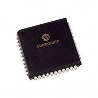
PIC18C442-E/L Microchip Technology, PIC18C442-E/L Datasheet - Page 87

PIC18C442-E/L
Manufacturer Part Number
PIC18C442-E/L
Description
IC MCU OTP 8KX16 A/D 44PLCC
Manufacturer
Microchip Technology
Series
PIC® 18Cr
Datasheets
1.PIC16F616T-ISL.pdf
(8 pages)
2.PIC16C770-ISO.pdf
(8 pages)
3.PIC18C242-ISO.pdf
(305 pages)
4.PIC18C242-ISO.pdf
(12 pages)
Specifications of PIC18C442-E/L
Core Processor
PIC
Core Size
8-Bit
Speed
40MHz
Connectivity
I²C, SPI, UART/USART
Peripherals
Brown-out Detect/Reset, LVD, POR, PWM, WDT
Number Of I /o
33
Program Memory Size
16KB (8K x 16)
Program Memory Type
OTP
Ram Size
512 x 8
Voltage - Supply (vcc/vdd)
4.2 V ~ 5.5 V
Data Converters
A/D 8x10b
Oscillator Type
External
Operating Temperature
-40°C ~ 125°C
Package / Case
44-PLCC
For Use With
DVA16XL441 - ADAPTER DEVICE ICE 44PLCC
Lead Free Status / RoHS Status
Lead free / RoHS Compliant
Eeprom Size
-
Other names
PIC18C442E/L
Available stocks
Company
Part Number
Manufacturer
Quantity
Price
Company:
Part Number:
PIC18C442-E/L
Manufacturer:
Microchip Technology
Quantity:
10 000
- PIC16F616T-ISL PDF datasheet
- PIC16C770-ISO PDF datasheet #2
- PIC18C242-ISO PDF datasheet #3
- PIC18C242-ISO PDF datasheet #4
- Current page: 87 of 305
- Download datasheet (6Mb)
8.4
This section is only applicable to the PIC18C4X2
devices.
PORTD is an 8-bit wide, bi-directional port. The corre-
sponding Data Direction register is TRISD. Setting a
TRISD bit (= 1) will make the corresponding PORTD
pin an input (i.e., put the corresponding output driver in
a Hi-Impedance mode). Clearing a TRISD bit (= 0) will
make the corresponding PORTD pin an output (i.e., put
the contents of the output latch on the selected pin).
The Data Latch register (LATD) is also memory
mapped. Read-modify-write operations on the LATD
register reads and writes the latched output value for
PORTD.
PORTD is an 8-bit port with Schmitt Trigger input buff-
ers. Each pin is individually configurable as an input or
output.
PORTD can be configured as an 8-bit wide micropro-
cessor port (parallel slave port) by setting control bit
PSPMODE (TRISE<4>). In this mode, the input buffers
are TTL. See Section 8.6 for additional information on
the Parallel Slave Port (PSP).
EXAMPLE 8-4:
Note:
2001 Microchip Technology Inc.
CLRF
CLRF
MOVLW 0xCF
MOVWF TRISD
PORTD, TRISD and LATD
Registers
PORTD
LATD
On a Power-on Reset, these pins are con-
figured as digital inputs.
; Initialize PORTD by
; clearing output
; data latches
; Alternate method
; to clear output
; data latches
; Value used to
; initialize data
; direction
; Set RD<3:0> as inputs
; RD<5:4> as outputs
; RD<7:6> as inputs
INITIALIZING PORTD
FIGURE 8-8:
WR TRISD
WR LATD
or
PORTD
Data
Bus
Note 1: I/O pins have diode protection to V
RD PORTD
TRIS Latch
Data Latch
RD LATD
D
D
CK
CK
RD TRISD
Q
PORTD BLOCK DIAGRAM
IN I/O PORT MODE
Q
PIC18CXX2
Q
EN
EN
Schmitt
Trigger
Input
Buffer
D
DS39026C-page 85
DD
and V
SS
I/O pin
.
(1)
Related parts for PIC18C442-E/L
Image
Part Number
Description
Manufacturer
Datasheet
Request
R

Part Number:
Description:
IC, 8BIT MCU, PIC18F, 40MHZ, LCC-44
Manufacturer:
Microchip Technology
Datasheet:

Part Number:
Description:
IC, 8BIT MCU, PIC18LF, 40MHZ, PLCC-64
Manufacturer:
Microchip Technology
Datasheet:

Part Number:
Description:
IC, 8BIT MCU, PIC18F, 64MHZ, TQFP-80
Manufacturer:
Microchip Technology
Datasheet:

Part Number:
Description:
MCU, MPU & DSP Development Tools CAN/LIN PICtail Plus Daughter Board
Manufacturer:
Microchip Technology
Datasheet:

Part Number:
Description:
IC, 8BIT MCU, PIC18F, 64MHZ, DIP-40
Manufacturer:
Microchip Technology
Datasheet:

Part Number:
Description:
IC, 8BIT MCU, PIC18LF, 40MHZ, PLCC-64
Manufacturer:
Microchip Technology
Datasheet:

Part Number:
Description:
IC, 8BIT MCU, PIC18F, 64MHZ, TQFP-64
Manufacturer:
Microchip Technology

Part Number:
Description:
IC, 8BIT MCU, PIC18F, 64MHZ, TQFP-80
Manufacturer:
Microchip Technology

Part Number:
Description:
8KB, Flash, 768bytes-RAM, 36I/O, 8-bit Family,nanowatt XLP 40 UQFN 5x5x0.5mm TUB
Manufacturer:
Microchip Technology
Datasheet:

Part Number:
Description:
8KB, Flash, 768bytes-RAM, 36I/O, 8-bit Family,nanowatt XLP 40 UQFN 5x5x0.5mm TUB
Manufacturer:
Microchip Technology

Part Number:
Description:
16KB, Flash, 768bytes-RAM, 36I/O, 8-bit Family,nanowatt XLP 40 UQFN 5x5x0.5mm TU
Manufacturer:
Microchip Technology
Datasheet:

Part Number:
Description:
16KB, Flash, 768bytes-RAM, 36I/O, 8-bit Family,nanowatt XLP 40 UQFN 5x5x0.5mm TU
Manufacturer:
Microchip Technology

Part Number:
Description:
32KB, Flash, 1536bytes-RAM, 36I/O, 8-bit Family,nanowatt XLP 40 UQFN 5x5x0.5mm T
Manufacturer:
Microchip Technology
Datasheet:

Part Number:
Description:
32KB, Flash, 1536bytes-RAM, 36I/O, 8-bit Family,nanowatt XLP 40 UQFN 5x5x0.5mm T
Manufacturer:
Microchip Technology

Part Number:
Description:
64KB, Flash, 3968bytes-RAM, 36I/O, 8-bit Family,nanowatt XLP 40 UQFN 5x5x0.5mm T
Manufacturer:
Microchip Technology
Datasheet:


