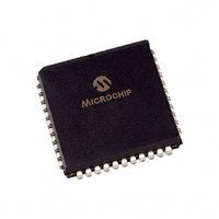
PIC18C442-E/L Microchip Technology, PIC18C442-E/L Datasheet - Page 92

PIC18C442-E/L
Manufacturer Part Number
PIC18C442-E/L
Description
IC MCU OTP 8KX16 A/D 44PLCC
Manufacturer
Microchip Technology
Series
PIC® 18Cr
Datasheets
1.PIC16F616T-ISL.pdf
(8 pages)
2.PIC16C770-ISO.pdf
(8 pages)
3.PIC18C242-ISO.pdf
(305 pages)
4.PIC18C242-ISO.pdf
(12 pages)
Specifications of PIC18C442-E/L
Core Processor
PIC
Core Size
8-Bit
Speed
40MHz
Connectivity
I²C, SPI, UART/USART
Peripherals
Brown-out Detect/Reset, LVD, POR, PWM, WDT
Number Of I /o
33
Program Memory Size
16KB (8K x 16)
Program Memory Type
OTP
Ram Size
512 x 8
Voltage - Supply (vcc/vdd)
4.2 V ~ 5.5 V
Data Converters
A/D 8x10b
Oscillator Type
External
Operating Temperature
-40°C ~ 125°C
Package / Case
44-PLCC
For Use With
DVA16XL441 - ADAPTER DEVICE ICE 44PLCC
Lead Free Status / RoHS Status
Lead free / RoHS Compliant
Eeprom Size
-
Other names
PIC18C442E/L
Available stocks
Company
Part Number
Manufacturer
Quantity
Price
Company:
Part Number:
PIC18C442-E/L
Manufacturer:
Microchip Technology
Quantity:
10 000
- PIC16F616T-ISL PDF datasheet
- PIC16C770-ISO PDF datasheet #2
- PIC18C242-ISO PDF datasheet #3
- PIC18C242-ISO PDF datasheet #4
- Current page: 92 of 305
- Download datasheet (6Mb)
PIC18CXX2
8.6
The Parallel Slave Port is implemented on the 40-pin
devices only (PIC18C4X2).
PORTD operates as an 8-bit wide, parallel slave port,
or microprocessor port, when control bit PSPMODE
(TRISE<4>) is set. It is asynchronously readable and
writable by the external world through RD control input
pin RE0/RD and WR control input pin RE1/WR.
It can directly interface to an 8-bit microprocessor data
bus. The external microprocessor can read or write the
PORTD latch as an 8-bit latch. Setting bit PSPMODE
enables port pin RE0/RD to be the RD input, RE1/WR
to be the WR input and RE2/CS to be the CS (chip
select) input. For this functionality, the corresponding
data direction bits of the TRISE register (TRISE<2:0>)
must be configured as inputs (set). The A/D port config-
uration bits PCFG2:PCFG0 (ADCON1<2:0>) must be
set, which will configure pins RE2:RE0 as digital I/O.
A write to the PSP occurs when both the CS and WR
lines are first detected low. A read from the PSP occurs
when both the CS and RD lines are first detected low.
The PORTE I/O pins become control inputs for the
microprocessor port when bit PSPMODE (TRISE<4>)
is set. In this mode, the user must make sure that the
TRISE<2:0> bits are set (pins are configured as digital
inputs), and the ADCON1 is configured for digital I/O.
In this mode, the input buffers are TTL.
FIGURE 8-11:
DS39026C-page 90
PORTD<7:0>
PSPIF
Parallel Slave Port
OBF
CS
WR
RD
IBF
Q1
PARALLEL SLAVE PORT WRITE WAVEFORMS
Q2
Q3
Q4
Q1
Q2
FIGURE 8-10:
One bit of PORTD
Data Bus
Q3
Set Interrupt Flag
PSPIF (PIR1<7>)
Note: I/O pin has protection diodes to V
WR LATD
or
PORTD
RD PORTD
RD LATD
Q4
Data Latch
Q
D
CK
Q1
EN
EN
Q
D
PORTD AND PORTE
BLOCK DIAGRAM
(PARALLEL SLAVE
PORT)
2001 Microchip Technology Inc.
Q2
Chip Select
Read
Write
Q3
TTL
TTL
TTL
TTL
DD
Q4
and V
SS
RDx
pin
RD
CS
WR
.
Related parts for PIC18C442-E/L
Image
Part Number
Description
Manufacturer
Datasheet
Request
R

Part Number:
Description:
IC, 8BIT MCU, PIC18F, 40MHZ, LCC-44
Manufacturer:
Microchip Technology
Datasheet:

Part Number:
Description:
IC, 8BIT MCU, PIC18LF, 40MHZ, PLCC-64
Manufacturer:
Microchip Technology
Datasheet:

Part Number:
Description:
IC, 8BIT MCU, PIC18F, 64MHZ, TQFP-80
Manufacturer:
Microchip Technology
Datasheet:

Part Number:
Description:
MCU, MPU & DSP Development Tools CAN/LIN PICtail Plus Daughter Board
Manufacturer:
Microchip Technology
Datasheet:

Part Number:
Description:
IC, 8BIT MCU, PIC18F, 64MHZ, DIP-40
Manufacturer:
Microchip Technology
Datasheet:

Part Number:
Description:
IC, 8BIT MCU, PIC18LF, 40MHZ, PLCC-64
Manufacturer:
Microchip Technology
Datasheet:

Part Number:
Description:
IC, 8BIT MCU, PIC18F, 64MHZ, TQFP-64
Manufacturer:
Microchip Technology

Part Number:
Description:
IC, 8BIT MCU, PIC18F, 64MHZ, TQFP-80
Manufacturer:
Microchip Technology

Part Number:
Description:
8KB, Flash, 768bytes-RAM, 36I/O, 8-bit Family,nanowatt XLP 40 UQFN 5x5x0.5mm TUB
Manufacturer:
Microchip Technology
Datasheet:

Part Number:
Description:
8KB, Flash, 768bytes-RAM, 36I/O, 8-bit Family,nanowatt XLP 40 UQFN 5x5x0.5mm TUB
Manufacturer:
Microchip Technology

Part Number:
Description:
16KB, Flash, 768bytes-RAM, 36I/O, 8-bit Family,nanowatt XLP 40 UQFN 5x5x0.5mm TU
Manufacturer:
Microchip Technology
Datasheet:

Part Number:
Description:
16KB, Flash, 768bytes-RAM, 36I/O, 8-bit Family,nanowatt XLP 40 UQFN 5x5x0.5mm TU
Manufacturer:
Microchip Technology

Part Number:
Description:
32KB, Flash, 1536bytes-RAM, 36I/O, 8-bit Family,nanowatt XLP 40 UQFN 5x5x0.5mm T
Manufacturer:
Microchip Technology
Datasheet:

Part Number:
Description:
32KB, Flash, 1536bytes-RAM, 36I/O, 8-bit Family,nanowatt XLP 40 UQFN 5x5x0.5mm T
Manufacturer:
Microchip Technology

Part Number:
Description:
64KB, Flash, 3968bytes-RAM, 36I/O, 8-bit Family,nanowatt XLP 40 UQFN 5x5x0.5mm T
Manufacturer:
Microchip Technology
Datasheet:


