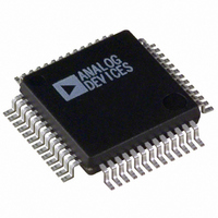
ADUC836BS Analog Devices Inc, ADUC836BS Datasheet - Page 34

ADUC836BS
Manufacturer Part Number
ADUC836BS
Description
IC ADC DUAL 16BIT W/MCU 52-MQFP
Manufacturer
Analog Devices Inc
Series
MicroConverter® ADuC8xxr
Datasheet
1.ADUC836BSZ.pdf
(80 pages)
Specifications of ADUC836BS
Rohs Status
RoHS non-compliant
Core Processor
8052
Core Size
8-Bit
Speed
12.58MHz
Connectivity
EBI/EMI, I²C, SPI, UART/USART
Peripherals
POR, PSM, PWM, Temp Sensor, WDT
Number Of I /o
34
Program Memory Size
62KB (62K x 8)
Program Memory Type
FLASH
Eeprom Size
4K x 8
Ram Size
2.25K x 8
Voltage - Supply (vcc/vdd)
2.7 V ~ 5.25 V
Data Converters
A/D 7x16b; D/A 1x12b
Oscillator Type
Internal
Operating Temperature
-40°C ~ 125°C
Package / Case
52-MQFP, 52-PQFP
Available stocks
Company
Part Number
Manufacturer
Quantity
Price
Company:
Part Number:
ADUC836BS
Manufacturer:
ADI
Quantity:
250
Part Number:
ADUC836BS
Manufacturer:
ADI/亚德诺
Quantity:
20 000
Company:
Part Number:
ADUC836BSZ
Manufacturer:
ADI
Quantity:
150
Company:
Part Number:
ADUC836BSZ
Manufacturer:
Analog Devices Inc
Quantity:
10 000
Part Number:
ADUC836BSZ
Manufacturer:
ADI/亚德诺
Quantity:
20 000
DAC
The ADuC836 incorporates a 12-bit voltage output DAC
on-chip. It has a rail-to-rail voltage output buffer capable of driving
10 k/100 pF. It has two selectable ranges, 0 V to V
nal band gap 2.5 V reference) and 0 V to AV
in 12-bit or 8-bit mode.The DAC has a control register, DACCON,
and two data registers, DACH/L. The DAC output can be
Bit
7
6
5
4
3
2
1
0
DACH/L
Function
SFR Address
Power-On Default Value
Bit Addressable
Using the D/A Converter
The on-chip D/A converter architecture consists of a resistor
string DAC followed by an output buffer amplifier, the functional
equivalent of which is illustrated in Figure 21.
ADuC836
Figure 21. Resistor String DAC Functional Equivalent
AV
V
Name
–––
–––
–––
DACPIN
DAC8
DACRN
DACCLR
DACEN
REF
DD
R
R
R
R
R
Description
Reserved for Future Use
Reserved for Future Use
Reserved for Future Use
DAC Output Pin Select.
Set by user to direct the DAC output to Pin 12 (P1.7/AIN4/DAC).
Cleared by user to direct the DAC output to Pin 3 (P1.2/DAC/IEXC1).
DAC 8-bit Mode Bit.
Set by user to enable 8-bit DAC operation. In this mode, the 8 bits in DACL SFR are routed to the 8 MSBs
of the DAC, and the 4 LSBs of the DAC are set to zero.
Cleared by user to operate the DAC in its normal 12-bit mode of operation.
DAC Output Range Bit.
Set by user to configure DAC range of 0 to AV
Cleared by user to configure DAC range of 0 V to 2.5 V (V
DAC Clear Bit.
Set to 1 by user to enable normal DAC operation.
Cleared to 0 by user to reset DAC data registers DACL/H to zero.
DAC Enable Bit.
Set to 1 by user to enable normal DAC operation.
Cleared to 0 by user to power down the DAC.
DAC Data Registers
DAC Data Registers, written by user to update the DAC output.
DACL (DAC Data Low Byte)
DACH (DAC Data High Byte)
00H
No
ADuC836
(FROM MCU)
OUTPUT
BUFFER
DISABLE
HIGH-Z
DD
Table XV. DACCON SFR Bit Designations
12
. It can operate
DAC
REF
(the inter-
FBH
FCH
Both Registers
Both Registers
–34–
programmed to appear at Pin 3 or Pin 12. It should be noted
that in 12-bit mode, the DAC voltage output will be updated
as soon as the DACL data SFR has been written; therefore, the
DAC data registers should be updated as DACH first, followed
by DACL. The 12-bit DAC data should be written into DACH/L
right-justified such that DACL contains the lower eight bits, and
the lower nibble of DACH contains the upper four bits.
Features of this architecture include inherent guaranteed monoto-
nicity and excellent differential linearity. As illustrated in Figure 21,
the reference source for the DAC is user selectable in software. It
can be either AV
transfer function spans from 0 V to the voltage at the AV
In 0-to-V
0 V to the internal V
features a true rail-to-rail output stage implementation.This means
that, unloaded, each output is capable of swinging to within less than
100 mV of both AV
ity specification (when driving a 10 k resistive load to ground)
is guaranteed through the full transfer function except codes 0
to 48 in 0-to-V
V
Linearity degradation near ground and V
of the output amplifier, and a general representation of its effects
(neglecting offset and gain error) is illustrated in Figure 22. The
dotted line in Figure 22 indicates the ideal transfer function, and
the solid line represents what the transfer function might look
like with endpoint nonlinearities due to saturation of the output
amplifier.
DD
DD
.
mode.
REF
mode, the DAC output transfer function spans from
REF
REF
DD
).
mode and 0 to 100 and 3950 to 4095 in 0-to-
or V
REF
DD
and ground. Moreover, the DAC’s linear-
REF
(2.5 V).The DAC output buffer amplifier
. In 0-to-AV
DD
DD
mode, the DAC output
is caused by saturation
DD
pin.
REV. A


