MC68HC705SR3CP Freescale Semiconductor, MC68HC705SR3CP Datasheet - Page 80
MC68HC705SR3CP
Manufacturer Part Number
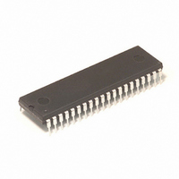
MC68HC705SR3CP
Description
IC MCU 3.75K 2.1MHZ OTP 40-DIP
Manufacturer
Freescale Semiconductor
Series
HC05r
Specifications of MC68HC705SR3CP
Core Processor
HC05
Core Size
8-Bit
Speed
4MHz
Peripherals
LED, POR
Number Of I /o
32
Program Memory Size
3.75KB (3.75K x 8)
Program Memory Type
OTP
Ram Size
192 x 8
Voltage - Supply (vcc/vdd)
3 V ~ 5.5 V
Data Converters
A/D 4x8b
Oscillator Type
Internal
Operating Temperature
-40°C ~ 85°C
Package / Case
40-DIP (0.600", 15.24mm)
Lead Free Status / RoHS Status
Contains lead / RoHS non-compliant
Eeprom Size
-
Connectivity
-
Available stocks
Company
Part Number
Manufacturer
Quantity
Price
Company:

Part Number:
MC68HC705SR3CP
Manufacturer:
MOTOROLA
Quantity:
82
Part Number:
MC68HC705SR3CP
Manufacturer:
MOTCROLA
Quantity:
20 000
Part Number:
MC68HC705SR3CPE
Manufacturer:
FREESCALE
Quantity:
20 000


11
11.4
Freescale
11-4
Notes:
(1) Error includes quantization. ADC accuracy may decrease proportionately as V
(2) Source impedances greater than 10KΩ adversely affect internal RC charging time during input sampling.
(3) The external system error caused by input leakage current is approximately equal to the product of R source and input current.
Resolution
Absolute accuracy
Conversion range
Power-up time
V
V
Conversion time
Monotonicity
Zero-input reading
Full-scale reading
Sample acquisition time
Input capacitance
Input leakage
RH
RL
CHARACTERISTICS
Table 11-3 ADC Electrical Characteristics for 5V and 3V Operation
ADC Electrical Characteristics
Number of bits resolved by the ADC
Difference between the actual input voltage and the
full-scale equivalent of the binary code output code for all
errors.
Analog input voltage range
ADC power-up time delay, t
Maximum analog reference voltage
Minimum analog reference voltage
Total time to perform a single analog to digital conversion
(a) External clock (OSC1, OSC2)
(b) Internal RC oscillator
Conversion result never decreases with an increase in
input voltage and has no missing codes
Analog input acquisition sampling
(a) External clock (OSC1, OSC2)
(b) Internal RC oscillator
Input capacitance on AN0-AN3
Input leakage on ADC pins
AN0, AN1, AN2, AN3, V
Conversion result when V
Conversion result when V
(1)
ELECTRICAL SPECIFICATIONS
PARAMETER
RL
IN
IN
, V
(3)
=V
=V
ADON
RH
RL
RH
(2)
DD
is reduced below 3.0V.
MINIMUM
V
SS
V
V
00
—
—
—
—
—
Inherent (within total error)
—
—
—
—
—
8
RL
RL
–0.1
±1.5
±2
MAXIMUM
MC68HC05SR3
V
(V
DD
±400
V
V
500
32
32
FF
12
12
(V
DD
—
8
RH
RH
8
+0.1
DD
=3.3V)
=5V)
UNIT
LSB
LSB
t
t
t
bits
hex
hex
CYC
CYC
CYC
µs
µs
nA
pF
V
V
V
TPG
Related parts for MC68HC705SR3CP
Image
Part Number
Description
Manufacturer
Datasheet
Request
R

Part Number:
Description:
Manufacturer:
Freescale Semiconductor, Inc
Datasheet:
Part Number:
Description:
Manufacturer:
Freescale Semiconductor, Inc
Datasheet:
Part Number:
Description:
Manufacturer:
Freescale Semiconductor, Inc
Datasheet:
Part Number:
Description:
Manufacturer:
Freescale Semiconductor, Inc
Datasheet:
Part Number:
Description:
Manufacturer:
Freescale Semiconductor, Inc
Datasheet:
Part Number:
Description:
Manufacturer:
Freescale Semiconductor, Inc
Datasheet:
Part Number:
Description:
Manufacturer:
Freescale Semiconductor, Inc
Datasheet:
Part Number:
Description:
Manufacturer:
Freescale Semiconductor, Inc
Datasheet:
Part Number:
Description:
Manufacturer:
Freescale Semiconductor, Inc
Datasheet:
Part Number:
Description:
Manufacturer:
Freescale Semiconductor, Inc
Datasheet:
Part Number:
Description:
Manufacturer:
Freescale Semiconductor, Inc
Datasheet:
Part Number:
Description:
Manufacturer:
Freescale Semiconductor, Inc
Datasheet:
Part Number:
Description:
Manufacturer:
Freescale Semiconductor, Inc
Datasheet:
Part Number:
Description:
Manufacturer:
Freescale Semiconductor, Inc
Datasheet:
Part Number:
Description:
Manufacturer:
Freescale Semiconductor, Inc
Datasheet: