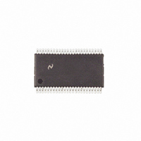
COP8SCR9IMT8 National Semiconductor, COP8SCR9IMT8 Datasheet - Page 18

COP8SCR9IMT8
Manufacturer Part Number
COP8SCR9IMT8
Description
IC MCU EEPROM 8BIT 32K 48-TSSOP
Manufacturer
National Semiconductor
Series
COP8™ 8Sr
Datasheet
1.COP8SCR9HVA8NOPB.pdf
(80 pages)
Specifications of COP8SCR9IMT8
Core Processor
COP8
Core Size
8-Bit
Speed
20MHz
Connectivity
Microwire/Plus (SPI), UART/USART
Peripherals
Brown-out Detect/Reset, POR, PWM, WDT
Number Of I /o
39
Program Memory Size
32KB (32K x 8)
Program Memory Type
FLASH
Ram Size
1K x 8
Voltage - Supply (vcc/vdd)
2.7 V ~ 5.5 V
Oscillator Type
Internal
Operating Temperature
-40°C ~ 85°C
Package / Case
48-TSSOP
Lead Free Status / RoHS Status
Contains lead / RoHS non-compliant
Eeprom Size
-
Data Converters
-
Other names
*COP8SCR9IMT8
www.national.com
9.0 Pin Descriptions
Writing a “1” to bit 6 of the Port G Configuration Register
enables the MICROWIRE/PLUS to operate with the alter-
nate phase of the SK clock. The G7 configuration bit, if set
high, enables the clock start up delay after HALT when the
R/C clock configuration is used.
Port G has the following alternate features:
G7 CKO Oscillator dedicated output
G6 SI (MICROWIRE/PLUS Serial Data Input)
G5 SK (MICROWIRE/PLUS Serial Clock)
G4 SO (MICROWIRE/PLUS Serial Data Output)
G3 T1A (Timer T1 I/O)
G2 T1B (Timer T1 Capture Input)
G1 WDOUT WATCHDOG and/or Clock Monitor if WATCH-
G0 INTR (External Interrupt Input)
G0 through G3 are also used for In-System Emulation.
Port L is an 8-bit I/O port. All L-pins have Schmitt triggers on
the inputs.
Port L supports the Multi-Input Wake-Up feature on all eight
pins. Port L has the following alternate pin functions:
L7 Multi-Input Wake-up or T3B (Timer T3B Input)
L6 Multi-Input Wake-up or T3A (Timer T3A Input/Output)
L5 Multi-Input Wake-up or T2B (Timer T2B Input)
L4 Multi-Input Wake-up or T2A (Timer T2A Input/Output)
L3 Multi-Input Wake-up and/or RDX (USART Receive)
L2 Multi-Input Wake-up or TDX (USART Transmit)
L1 Multi-Input Wake-up and/or CKX (USART Clock) (Low
L0 Multi-Input Wake-up (Low Speed Oscillator Input)
Port D is an 8-bit output port that is preset high when RESET
goes low. The user can tie two or more D port outputs
(except D2) together in order to get a higher drive.
Note: Care must be exercised with the D2 pin operation. At
RESET, the external loads on this pin must ensure that the
output voltages stay above 0.7 V
entering special modes. Also keep the external loading on
D2 to less than 1000 pF.
Speed Oscillator Output)
DOG enabled, otherwise it is a general purpose I/O
G7
G6
FIGURE 3. I/O Port Configurations
CLKDLY
Alternate SK
Config. Reg.
CC
to prevent the chip from
(Continued)
HALT
IDLE
Data Reg.
10138906
18
9.1 EMULATION CONNECTION
Connection to the emulation system is made via a 2 x 7
connector which interrupts the continuity of the RESET, G0,
G1, G2 and G3 signals between the COP8 device and the
rest of the target system (as shown in Figure 6). This con-
nector can be designed into the production pc board and can
be replaced by jumpers or signal traces when emulation is
no longer necessary. The emulator will replicate all functions
of G0 - G3 and RESET. For proper operation, no connection
should be made on the device side of the emulator connec-
tor.
FIGURE 4. I/O Port Configurations — Output Mode
FIGURE 5. I/O Port Configurations — Input Mode
10138908
10138907


