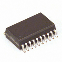
MC68HC908JB16JDW Freescale Semiconductor, MC68HC908JB16JDW Datasheet - Page 273

MC68HC908JB16JDW
Manufacturer Part Number
MC68HC908JB16JDW
Description
IC MCU 16K FLASH 6MHZ USB 20SOIC
Manufacturer
Freescale Semiconductor
Series
HC08r
Datasheet
1.MC908JB16DWE.pdf
(332 pages)
Specifications of MC68HC908JB16JDW
Core Processor
HC08
Core Size
8-Bit
Speed
6MHz
Connectivity
SCI, USB
Peripherals
LED, LVD, POR, PWM
Number Of I /o
13
Program Memory Size
16KB (16K x 8)
Program Memory Type
FLASH
Ram Size
384 x 8
Voltage - Supply (vcc/vdd)
4 V ~ 5.5 V
Oscillator Type
Internal
Operating Temperature
0°C ~ 70°C
Package / Case
20-SOIC (7.5mm Width)
Lead Free Status / RoHS Status
Contains lead / RoHS non-compliant
Eeprom Size
-
Data Converters
-
Available stocks
Company
Part Number
Manufacturer
Quantity
Price
Part Number:
MC68HC908JB16JDWE
Manufacturer:
FREESCALE
Quantity:
20 000
- Current page: 273 of 332
- Download datasheet (4Mb)
14.5.2 Data Direction Register D
MC68HC908JB16
Freescale Semiconductor
NOTE:
NOTE:
—
Rev. 1.1
Address:
Data direction register D determines whether each port D pin is an input
or an output. Writing a logic 1 to a DDRD bit enables the output buffer for
the corresponding port D pin; a logic 0 disables the output buffer.
DDRD[5:0] — Data Direction Register D Bits
Avoid glitches on port D pins by writing to the port D data register before
changing data direction register D bits from 0 to 1.
For those devices packaged in a 32-pin low-profile quad flat pack,
PTD5–1 are not connected. DDRD5–1 should be set to a 1 to configure
PTD5–1 as outputs.
Figure 14-10
Reset:
Read:
Write:
These read/write bits control port D data direction. Reset clears
DDRD[5:0], configuring all port D pins as inputs.
Port D pins are open-drain when configured as output.
1 = Corresponding port D pin configured as output
0 = Corresponding port D pin configured as input
$0007
Bit 7
0
0
Figure 14-9. Data Direction Register D (DDRD)
shows the port D I/O circuit logic.
Input/Output (I/O) Ports
6
0
0
DDRD5
5
0
DDRD4
4
0
DDRD3
3
0
DDRD2
2
0
Input/Output (I/O) Ports
DDRD1
1
0
Technical Data
DDRD0
Bit 0
0
273
Related parts for MC68HC908JB16JDW
Image
Part Number
Description
Manufacturer
Datasheet
Request
R
Part Number:
Description:
Manufacturer:
Freescale Semiconductor, Inc
Datasheet:
Part Number:
Description:
Manufacturer:
Freescale Semiconductor, Inc
Datasheet:
Part Number:
Description:
Manufacturer:
Freescale Semiconductor, Inc
Datasheet:
Part Number:
Description:
Manufacturer:
Freescale Semiconductor, Inc
Datasheet:
Part Number:
Description:
Manufacturer:
Freescale Semiconductor, Inc
Datasheet:
Part Number:
Description:
Manufacturer:
Freescale Semiconductor, Inc
Datasheet:
Part Number:
Description:
Manufacturer:
Freescale Semiconductor, Inc
Datasheet:
Part Number:
Description:
Manufacturer:
Freescale Semiconductor, Inc
Datasheet:
Part Number:
Description:
Manufacturer:
Freescale Semiconductor, Inc
Datasheet:
Part Number:
Description:
Manufacturer:
Freescale Semiconductor, Inc
Datasheet:
Part Number:
Description:
Manufacturer:
Freescale Semiconductor, Inc
Datasheet:
Part Number:
Description:
Manufacturer:
Freescale Semiconductor, Inc
Datasheet:
Part Number:
Description:
Manufacturer:
Freescale Semiconductor, Inc
Datasheet:
Part Number:
Description:
Manufacturer:
Freescale Semiconductor, Inc
Datasheet:
Part Number:
Description:
Manufacturer:
Freescale Semiconductor, Inc
Datasheet:


