C8051F350 Silicon Laboratories Inc, C8051F350 Datasheet - Page 113
C8051F350
Manufacturer Part Number
C8051F350
Description
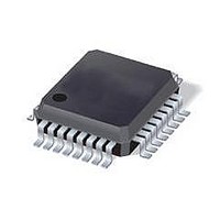
IC 8051 MCU 8K FLASH 32LQFP
Manufacturer
Silicon Laboratories Inc
Series
C8051F35xr
Specifications of C8051F350
Core Processor
8051
Core Size
8-Bit
Speed
50MHz
Connectivity
SMBus (2-Wire/I²C), SPI, UART/USART
Peripherals
POR, PWM, Temp Sensor, WDT
Number Of I /o
17
Program Memory Size
8KB (8K x 8)
Program Memory Type
FLASH
Ram Size
768 x 8
Voltage - Supply (vcc/vdd)
2.7 V ~ 3.6 V
Data Converters
A/D 8x24b; D/A 2x8b
Oscillator Type
Internal
Operating Temperature
-40°C ~ 85°C
Package / Case
32-LQFP
Data Bus Width
8 bit
Data Rom Size
128 B
On-chip Adc
10 bit
Number Of Timers
16 bit
Operating Supply Voltage
2.7 V to 3.6 V
Mounting Style
SMD/SMT
Height
1.4 mm
Length
7 mm
Maximum Operating Temperature
+ 85 C
Minimum Operating Temperature
- 40 C
Width
7 mm
Lead Free Status / RoHS Status
Contains lead / RoHS non-compliant
Eeprom Size
-
Lead Free Status / Rohs Status
No RoHS Version Available
Available stocks
Company
Part Number
Manufacturer
Quantity
Price
Company:

Part Number:
C8051F350
Manufacturer:
Silicon Laboratories Inc
Quantity:
10 000
Part Number:
C8051F350
Manufacturer:
SILICON LABS/èٹ¯ç§‘
Quantity:
20 000
Company:
Part Number:
C8051F350-GQ
Manufacturer:
SiliconL
Quantity:
3 029
Company:
Part Number:
C8051F350-GQ
Manufacturer:
SILICON
Quantity:
18
Company:
Part Number:
C8051F350-GQ
Manufacturer:
Silicon Laboratories Inc
Quantity:
10 000
Company:
Part Number:
C8051F350-GQR
Manufacturer:
Silicon Laboratories Inc
Quantity:
10 000
Part Number:
C8051F350-GQR
Manufacturer:
SILICON LABS/èٹ¯ç§‘
Quantity:
20 000
Company:
Part Number:
C8051F350DK
Manufacturer:
SiliconL
Quantity:
8
Company:
Part Number:
C8051F350R
Manufacturer:
Silicon Laboratories Inc
Quantity:
10 000


14.2. Power-Fail Reset /
When a power-down transition or power irregularity causes V
monitor will drive the /RST pin low and hold the CIP-51 in a reset state (see Figure 14.2). When V
returns to a level above V
nal data memory contents are not altered by the power-fail reset, it is impossible to determine if V
dropped below the level required for data retention. If the PORSF flag reads ‘1’, the data may no longer be
valid. The V
defined state (enabled/disabled) is not altered by any other reset source. For example, if the V
is disabled by software, and a software reset is performed, the V
reset. To protect the integrity of Flash contents, it is strongly recommended that the V
remain enabled and selected as a reset source if software contains routines which erase or write
Flash memory.
The V
reset source before it is enabled and stabilized may cause a system reset. The procedure for re-enabling
the V
See Figure 14.2 for V
See Table 14.1 for complete electrical characteristics of the V
Bit7:
Bit6:
Bits5-0:
VDMEN
DD
R/W
DD
Bit7
Step 1. Enable the V
Step 2. Wait for the V
Step 3. Select the V
monitor and configuring the V
monitor must be enabled before it is selected as a reset source. Selecting the V
Note: This delay should be omitted if software contains routines which erase or write
Flash memory.
VDMEN: V
This bit is turns the V
resets until it is also selected as a reset source in register RSTSRC (Figure 14.4). The V
Monitor must be allowed to stabilize before it is selected as a reset source. Selecting the
V
See Table 14.1 for the minimum V
0: V
1: V
V
This bit indicates the current power supply status (V
0: V
1: V
Reserved. Read = Variable. Write = don’t care.
DD
DD
DD
V
DD
DD
DD
DD
DD
monitor is enabled and selected as a reset source after power-on resets; however its
monitor as a reset source before it has stabilized may generate a system reset.
STAT: V
Bit6
R
STAT Reserved Reserved Reserved Reserved Reserved Reserved
Monitor Disabled.
Monitor Enabled (default).
is at or below the V
is above the V
DD
DD
monitor timing; note that the reset delay is not incurred after a V
DD
RST
Figure 14.3. VDM0CN:
Monitor Enable.
Status.
DD
Bit5
, the CIP-51 will be released from the reset state. Note that even though inter-
DD
R
DD
monitor as a reset source (PORSF bit in RSTSRC = ‘1’).
V
monitor (VDMEN bit in VDM0CN = ‘1’).
monitor to stabilize (see Table 14.1 for the V
DD
DD
DD
monitor circuit on/off. The V
Monitor
monitor threshold.
DD
DD
Bit4
R
monitor as a reset source is shown below:
monitor threshold.
DD
Rev. 0.4
Monitor turn-on time.
Bit3
R
V
DD
Monitor Control
DD
Bit2
DD
R
DD
DD
monitor.
DD
to drop below V
Monitor output).
Monitor cannot generate system
monitor will still be disabled after the
C8051F350/1/2/3
Bit1
R
DD
Monitor turn-on time).
SFR Address:
RST
Bit0
R
, the power supply
DD
DD
monitor reset.
0xFF
monitor as a
Reset Value
DD
Variable
DD
monitor
monitor
DD
113
DD
DD
Related parts for C8051F350
Image
Part Number
Description
Manufacturer
Datasheet
Request
R

Part Number:
Description:
SMD/C°/SINGLE-ENDED OUTPUT SILICON OSCILLATOR
Manufacturer:
Silicon Laboratories Inc
Part Number:
Description:
Manufacturer:
Silicon Laboratories Inc
Datasheet:
Part Number:
Description:
N/A N/A/SI4010 AES KEYFOB DEMO WITH LCD RX
Manufacturer:
Silicon Laboratories Inc
Datasheet:
Part Number:
Description:
N/A N/A/SI4010 SIMPLIFIED KEY FOB DEMO WITH LED RX
Manufacturer:
Silicon Laboratories Inc
Datasheet:
Part Number:
Description:
N/A/-40 TO 85 OC/EZLINK MODULE; F930/4432 HIGH BAND (REV E/B1)
Manufacturer:
Silicon Laboratories Inc
Part Number:
Description:
EZLink Module; F930/4432 Low Band (rev e/B1)
Manufacturer:
Silicon Laboratories Inc
Part Number:
Description:
I°/4460 10 DBM RADIO TEST CARD 434 MHZ
Manufacturer:
Silicon Laboratories Inc
Part Number:
Description:
I°/4461 14 DBM RADIO TEST CARD 868 MHZ
Manufacturer:
Silicon Laboratories Inc
Part Number:
Description:
I°/4463 20 DBM RFSWITCH RADIO TEST CARD 460 MHZ
Manufacturer:
Silicon Laboratories Inc
Part Number:
Description:
I°/4463 20 DBM RADIO TEST CARD 868 MHZ
Manufacturer:
Silicon Laboratories Inc
Part Number:
Description:
I°/4463 27 DBM RADIO TEST CARD 868 MHZ
Manufacturer:
Silicon Laboratories Inc
Part Number:
Description:
I°/4463 SKYWORKS 30 DBM RADIO TEST CARD 915 MHZ
Manufacturer:
Silicon Laboratories Inc
Part Number:
Description:
N/A N/A/-40 TO 85 OC/4463 RFMD 30 DBM RADIO TEST CARD 915 MHZ
Manufacturer:
Silicon Laboratories Inc
Part Number:
Description:
I°/4463 20 DBM RADIO TEST CARD 169 MHZ
Manufacturer:
Silicon Laboratories Inc