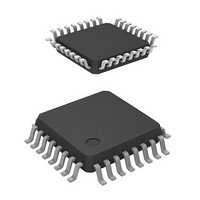
R5F21132FP Renesas Electronics America, R5F21132FP Datasheet - Page 10

R5F21132FP
Manufacturer Part Number
R5F21132FP
Description
IC R8C MCU FLASH 8K 32LQFP
Manufacturer
Renesas Electronics America
Series
M16C™ M16C/R8C/Tiny/13r
Datasheet
1.R5F21132FPU0.pdf
(33 pages)
Specifications of R5F21132FP
Core Processor
R8C
Core Size
16-Bit
Speed
20MHz
Connectivity
SIO, UART/USART
Peripherals
LED, POR, Voltage Detect, WDT
Number Of I /o
22
Program Memory Size
8KB (8K x 8)
Program Memory Type
FLASH
Ram Size
512 x 8
Voltage - Supply (vcc/vdd)
2.7 V ~ 5.5 V
Data Converters
A/D 12x10b
Oscillator Type
Internal
Operating Temperature
-20°C ~ 85°C
Package / Case
32-LQFP
For Use With
R0E521134CPE00 - EMULATOR COMPACT R8C/13
Lead Free Status / RoHS Status
Contains lead / RoHS non-compliant
Eeprom Size
-
Available stocks
Company
Part Number
Manufacturer
Quantity
Price
Company:
Part Number:
R5F21132FP#V0
Manufacturer:
Renesas Electronics America
Quantity:
10 000
R8C/13 Group
Rev.1.20
REJ03B0069-0120
2.2 Address Registers (A0 and A1)
2.3 Frame Base Register (FB)
2.4 Interrupt Table Register (INTB)
2.5 Program Counter (PC)
2.6 User Stack Pointer (USP) and Interrupt Stack Pointer (ISP)
2.7 Static Base Register (SB)
2.8 Flag Register (FLG)
A0 is a 16-bit register for address register indirect addressing and address register relative addressing.
They also are used for transfer, arithmetic and logic operations. The same applies to A1 as A0. A0 can be
combined with A0 to be used as a 32-bit address register (A1A0).
FB is a 16-bit register for FB relative addressing.
INTB is a 20-bit register indicates the start address of an interrupt vector table.
PC, 20 bits wide, indicates the address of an instruction to be executed.
The stack pointer (SP), USP and ISP, are 16 bits wide each.
The U flag of FLG is used to switch between USP and ISP.
SB is a 16-bit register for SB relative addressing.
FLG is a 11-bit register indicating the CPU state.
2.8.1 Carry Flag (C)
2.8.2 Debug Flag (D)
2.8.3 Zero Flag (Z)
2.8.4 Sign Flag (S)
2.8.5 Register Bank Select Flag (B)
2.8.6 Overflow Flag (O)
2.8.7 Interrupt Enable Flag (I)
2.8.8 Stack Pointer Select Flag (U)
2.8.9 Processor Interrupt Priority Level (IPL)
2.8.10 Reserved Bit
The C flag retains a carry, borrow, or shift-out bit that has occurred in the arithmetic logic unit.
The D flag is for debug only. Set to “0”.
The Z flag is set to “1” when an arithmetic operation resulted in 0; otherwise, “0”.
The S flag is set to “1” when an arithmetic operation resulted in a negative value; otherwise, “0”.
The register bank 0 is selected when the B flag is “0”. The register bank 1 is selected when this flag is
set to “1”.
The O flag is set to “1” when the operation resulted in an overflow; otherwise, “0”.
The I flag enables a maskable interrupt.
An interrupt is disabled when the I flag is set to “0”, and are enabled when the I flag is set to “1”. The
I flag is set to “0” when an interrupt request is acknowledged.
ISP is selected when the U flag is set to “0”, USP is selected when the U flag is set to “1”.
The U flag is set to “0” when a hardware interrupt request is acknowledged or the INT instruction of
software interrupt numbers 0 to 31 is executed.
IPL, 3 bits wide, assigns processor interrupt priority levels from level 0 to level 7.
If a requested interrupt has greater priority than IPL, the interrupt is enabled.
When write to this bit, set to “0”. When read, its content is indeterminate.
Jan 27, 2006
page 8 of 27
2. Central Processing Unit (CPU)


