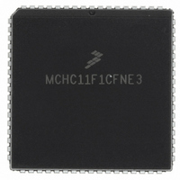
MCHC11F1CFNE3 Freescale Semiconductor, MCHC11F1CFNE3 Datasheet - Page 61

MCHC11F1CFNE3
Manufacturer Part Number
MCHC11F1CFNE3
Description
IC MCU 8BIT 1K RAM 68-PLCC
Manufacturer
Freescale Semiconductor
Series
HC11r
Specifications of MCHC11F1CFNE3
Core Processor
HC11
Core Size
8-Bit
Speed
3MHz
Connectivity
SCI, SPI
Peripherals
POR, WDT
Number Of I /o
30
Program Memory Type
ROMless
Eeprom Size
512 x 8
Ram Size
1K x 8
Voltage - Supply (vcc/vdd)
4.75 V ~ 5.25 V
Data Converters
A/D 8x8b
Oscillator Type
Internal
Operating Temperature
-40°C ~ 85°C
Package / Case
68-PLCC
A/d Inputs
8-Channel, 8-Bit
Eeprom Memory
512 Bytes
Input Output
30
Interface
SCI/SPI
Memory Type
EPROM
Number Of Bits
8
Package Type
68-pin PLCC
Programmable Memory
0 Bytes
Timers
3-16-bit
Voltage, Range
3-5.5 V
Controller Family/series
68HC11
No. Of I/o's
30
Eeprom Memory Size
512Byte
Ram Memory Size
1KB
Cpu Speed
3MHz
No. Of Timers
1
Embedded Interface Type
SCI, SPI
Rohs Compliant
Yes
Processor Series
HC11F
Core
HC11
Data Bus Width
8 bit
Program Memory Size
512 B
Data Ram Size
1 KB
Interface Type
SCI, SPI
Maximum Clock Frequency
3 MHz
Number Of Timers
1
Maximum Operating Temperature
+ 85 C
Mounting Style
SMD/SMT
Minimum Operating Temperature
- 40 C
On-chip Adc
8 bit, 8 Channel
Lead Free Status / RoHS Status
Lead free / RoHS Compliant
Program Memory Size
-
Lead Free Status / Rohs Status
RoHS Compliant part
Available stocks
Company
Part Number
Manufacturer
Quantity
Price
Company:
Part Number:
MCHC11F1CFNE3
Manufacturer:
FREESCALE
Quantity:
5 530
Company:
Part Number:
MCHC11F1CFNE3
Manufacturer:
FREESCALE
Quantity:
5 530
Company:
Part Number:
MCHC11F1CFNE3
Manufacturer:
Freescale Semiconductor
Quantity:
10 000
Company:
Part Number:
MCHC11F1CFNE3R
Manufacturer:
Freescale Semiconductor
Quantity:
10 000
TCTL2 — Timer Control 2
EDGxB, EDGxA — Input Capture Edge Control
TMSK1 — Timer Interrupt Mask 1
OCxI — Output Compare x Interrupt Enable
I4/O5I — Input Capture 4/Output Compare 5 Interrupt Enable
ICxI — Input Capture x Interrupt Enable
TFLG1 — Timer Interrupt Flag 1
MC68HC11F1/FC0
MC68HC11FTS/D
RESET:
RESET:
RESET:
Each EDGxB, EDGxA pair determines the polarity of the input signal on the corresponding ICx that will
trigger an input capture, as shown in Table 30. IC4 functions only if the I4/O5 bit in the PACTL register
is set.
Bits in TMSK1 correspond bit for bit with flag bits in TFLG1. Each bit that is set in TMSK1 enables the
corresponding interrupt source.
If the OCxI enable bit is set when the OCxF flag bit is set, a hardware interrupt sequence is requested.
When I4/O5 in PACTL is one, I4/O5I is the input capture 4 interrupt enable bit. When I4/O5 in PACTL
is zero, I4/O5I is the output compare 5 interrupt enable bit.
If the ICxI enable bit is set when the ICxF flag bit is set, a hardware interrupt sequence is requested.
Bits in TFLG1 are cleared by writing a one to the corresponding bit positions.
EDG4B
OC1F
OC1I
Bit 7
Bit 7
Bit 7
0
0
0
EDG4A
OMx
OC2F
OC2I
0
0
1
1
6
0
6
0
6
0
EDGxB
Freescale Semiconductor, Inc.
0
0
1
1
For More Information On This Product,
OLx
Table 30 Input Capture Configuration
EDG1B
0
1
0
1
OC3F
Table 29 Output Compare Actions
OC3I
5
0
5
0
5
0
Timer disconnected from output pin logic
Toggle OCx output line
Clear OCx output line to zero
Set OCx output line to one
Go to: www.freescale.com
Action Taken on Successful Compare
EDGxA
EDG1A
OC4F
OC4I
0
1
0
1
4
0
4
0
4
0
EDG2B
I4/O5F
I4/O5I
Capture disabled
Capture on rising edges only
Capture on falling edges only
Capture on any edge
3
0
3
0
3
0
Configuration
EDG2A
IC1F
IC1I
2
0
2
0
2
0
EDG3B
IC2F
IC2I
1
0
1
0
1
0
EDG3A
Bit 0
IC3F
Bit 0
Bit 0
IC3I
0
0
0
$x021
$x022
$x023
61


