M30263F6AFP#U9A Renesas Electronics America, M30263F6AFP#U9A Datasheet - Page 189
M30263F6AFP#U9A
Manufacturer Part Number
M30263F6AFP#U9A
Description
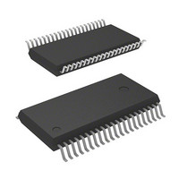
IC M16C/26A MCU FLASH 42-SSOP
Manufacturer
Renesas Electronics America
Series
M16C™ M16C/Tiny/26r
Datasheet
1.M30260F3AGPU5A.pdf
(354 pages)
Specifications of M30263F6AFP#U9A
Core Processor
M16C/60
Core Size
16-Bit
Speed
20MHz
Connectivity
I²C, IEBus, SIO, UART/USART
Peripherals
DMA, PWM, Voltage Detect, WDT
Number Of I /o
33
Program Memory Size
48KB (48K x 8)
Program Memory Type
FLASH
Ram Size
2K x 8
Voltage - Supply (vcc/vdd)
2.7 V ~ 5.5 V
Data Converters
A/D 10x10b
Oscillator Type
Internal
Operating Temperature
-20°C ~ 85°C
Package / Case
42-SSOP
For Use With
R0K33026AS000BE - KIT DEV EVALUATION M16C/26A
Lead Free Status / RoHS Status
Lead free / RoHS Compliant
Eeprom Size
-


R
R
M
e
E
1
. v
Table 13.1.4.2. Registers to Be Used and Settings in Special Mode 2
J
NOTE:
6
0
Register
U2TB
U2RB
U2BRG
U2MR
U2C0
U2C1
U2SMR
U2SMR2
U2SMR3
U2SMR4
2
C
9
0 .
B
2 /
1. Not all bits in the register are described above. Set those bits to “0” when writing to the registers in
0
0
6
2
(1)
(1)
A
0
(1)
F
Special Mode 2.
2
e
G
0 -
b
o r
1 .
2
0
, 5
u
0 to 7
0 to 7
OER
0 to 7
SMD2 to SMD0
CKDIR
IOPOL
CLK1, CLK0
CRS
TXEPT
CRD
NCH
CKPOL
UFORM
TE
TI
RE
RI
U2IRS
U2RRM,
U2LCH, U2ERE
0 to 7
0 to 7
CKPH
NODC
0, 2, 4 to 7
0 to 7
0
p
2
0
(
M
0
Bit
7
1
6
C
page 170
2 /
6
, A
M
1
f o
6
Set transmission data
Reception data can be read
Overrun error flag
Set a transfer rate
Set to ‘001
Set this bit to “0” for master mode or “1” for slave mode
Set to “0”
Select the count source for the U2BRG register
Invalid because CRD = 1
Transmit register empty flag
Set to “1”
Select TxD2 pin output format
Clock phases can be set in combination with the CKPH bit in the U2SMR3
register
Set to “0”
Set this bit to “1” to enable transmission
Transmit buffer empty flag
Set this bit to “1” to enable reception
Reception complete flag
Select UART2 transmit interrupt cause
Set to “0”
Set to “0”
Set to “0”
Set to “0”
Set to “0”
Set to “0”
Clock phases can be set in combination with the CKPOL bit in the U2C0 register
C
3
2
2 /
9
6
, B
M
2
1
’
6
C
2 /
6
) T
Function
13. Serial I/O
Related parts for M30263F6AFP#U9A
Image
Part Number
Description
Manufacturer
Datasheet
Request
R

Part Number:
Description:
KIT STARTER FOR M16C/29
Manufacturer:
Renesas Electronics America
Datasheet:

Part Number:
Description:
KIT STARTER FOR R8C/2D
Manufacturer:
Renesas Electronics America
Datasheet:

Part Number:
Description:
R0K33062P STARTER KIT
Manufacturer:
Renesas Electronics America
Datasheet:

Part Number:
Description:
KIT STARTER FOR R8C/23 E8A
Manufacturer:
Renesas Electronics America
Datasheet:

Part Number:
Description:
KIT STARTER FOR R8C/25
Manufacturer:
Renesas Electronics America
Datasheet:

Part Number:
Description:
KIT STARTER H8S2456 SHARPE DSPLY
Manufacturer:
Renesas Electronics America
Datasheet:

Part Number:
Description:
KIT STARTER FOR R8C38C
Manufacturer:
Renesas Electronics America
Datasheet:

Part Number:
Description:
KIT STARTER FOR R8C35C
Manufacturer:
Renesas Electronics America
Datasheet:

Part Number:
Description:
KIT STARTER FOR R8CL3AC+LCD APPS
Manufacturer:
Renesas Electronics America
Datasheet:
Part Number:
Description:
KIT STARTER FOR RX610
Manufacturer:
Renesas Electronics America
Datasheet:

Part Number:
Description:
KIT STARTER FOR R32C/118
Manufacturer:
Renesas Electronics America
Datasheet:

Part Number:
Description:
KIT DEV RSK-R8C/26-29
Manufacturer:
Renesas Electronics America
Datasheet:

Part Number:
Description:
KIT STARTER FOR SH7124
Manufacturer:
Renesas Electronics America
Datasheet:

Part Number:
Description:
KIT STARTER FOR H8SX/1622
Manufacturer:
Renesas Electronics America
Datasheet:

Part Number:
Description:
KIT DEV FOR SH7203
Manufacturer:
Renesas Electronics America
Datasheet: