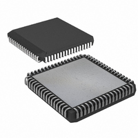
DS87C550-QNL Maxim Integrated Products, DS87C550-QNL Datasheet - Page 5

DS87C550-QNL
Manufacturer Part Number
DS87C550-QNL
Description
IC MCU EPROM ADC/PWM HS 68-PLCC
Manufacturer
Maxim Integrated Products
Series
87Cr
Datasheet
1.DS87C550-QNL.pdf
(49 pages)
Specifications of DS87C550-QNL
Core Processor
8051
Core Size
8-Bit
Speed
33MHz
Connectivity
EBI/EMI, SIO, UART/USART
Peripherals
Power-Fail Reset, PWM, WDT
Number Of I /o
55
Program Memory Size
8KB (8K x 8)
Program Memory Type
OTP
Ram Size
1K x 8
Voltage - Supply (vcc/vdd)
4.5 V ~ 5.5 V
Data Converters
A/D 6x10b
Oscillator Type
External
Operating Temperature
-40°C ~ 85°C
Package / Case
68-LCC, 68-PLCC
Lead Free Status / RoHS Status
Contains lead / RoHS non-compliant
Eeprom Size
-
Available stocks
Company
Part Number
Manufacturer
Quantity
Price
Company:
Part Number:
DS87C550-QNL
Manufacturer:
Maxim Integrated
Quantity:
10 000
Part Number:
DS87C550-QNL
Manufacturer:
DALLAS
Quantity:
20 000
PLCC/
CLCC
50-57
39-46
24-31
7-14
57
56
55
54
53
52
51
50
39
40
41
42
43
44
45
46
24
25
26
27
28
29
30
31
10
11
12
13
14
7
8
9
51-58
38-42
45-47
18-20
23-27
QFP
1-2
4-8
58
57
56
55
54
53
52
51
38
39
40
41
42
45
46
47
18
19
20
23
24
25
26
27
80
80
1
2
4
5
6
7
8
SIGNAL NAME
P0.0 (AD0)
P0.1 (AD1)
P0.2 (AD2)
P0.3 (AD3)
P0.4 (AD4)
P0.5 (AD5)
P0.6 (AD6)
P0.7 (AD7)
P2.2 (A10)
P2.3 (A11)
P2.4 (A12)
P2.5 (A13)
P2.6 (A14)
P2.7 (A15)
P2.0 (A8)
P2.1 (A9)
P3.0-P3.7
P4.0-P4.7
Port 0-I/O - AD0-7. Port 0 is an open-drain 8-bit, bi-directional general-purpose
I/O port. When used in this mode pullup resistors are required to provide a logic 1
output. As an alternate function, Port 0 operates as a multiplexed address/data bus
to access off-chip memory or peripherals. In this mode, the LSB of the memory
address is output on the bus during the time that ALE is high. When ALE falls to
a logic 0, the port transitions to a bi-directional data bus. In this mode, the port
provides active high drivers for logic 1 output. The reset condition of Port 0 is tri-
state (i.e., the open drain devices are off).
Port 2-I/O Address A15:A8. Port 2 functions as an 8-bit bi-directional I/O port
or alternately as an external address bus (A15-A8). The reset condition of Port 2 is
logic high I/O state. In this state, weak pullups hold the port high allowing the
pins to be used as an input or output as described above for Port 1. As an alternate
function Port 2 can function as MSB of the external address bus. This bus can be
used to read external memory or peripherals.
Port 3 - I/O. Port 3 functions as an 8-bit bi-directional I/O port or alternately as
an interface for External Interrupts, Serial Port 0, Timer 0 & 1 Inputs, and
above for Port 1. The alternate modes of Port 3 are detailed below.
Port
P3.0
P3.1
P3.2
P3.3
P3.4
P3.5
P3.6
P3.7
Port 4 - I/O. Port 4 functions as an 8-bit bi-directional I/O port or alternately as
an interface to Timer 2’s Capture Compare functions. When functioning as an I/O
port, these pins operate as indicated in the Port 1 description. The alternate modes
of Port 4 are detailed below.
Port 4 Alternate Mode
P4.0
P4.1
P4.2
P4.3
P4.4
P4.5
P4.6
P4.7
WR
strobes. When functioning as an I/O port, these pins operate as indicated
Alternate Mode
RXD0
TXD0
T0
T1
CMSR0
CMSR1
CMSR2
CMSR3
CMSR4
CMSR5
CMT0
CMT1
INT0
INT1
WR
RD
5 of 49
Serial Port 0 Input
Serial Port 0 Output
External Interrupt 0
External Interrupt 1
Timer 0 External Input
Timer 1 External Input
External Data Memory Write Strobe
External Data Memory Read Strobe
Timer 2 compare match set/reset output 0
Timer 2 compare match set/reset output 1
Timer 2 compare match set/reset output 2
Timer 2 compare match set/reset output 3
Timer 2 compare match set/reset output 4
Timer 2 compare match set/reset output 5
Timer 2 compare match toggle output 0
Timer 2 compare match toggle output 1
DESCRIPTION
RD
and


