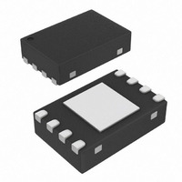
MCP6V06T-E/MNY Microchip Technology, MCP6V06T-E/MNY Datasheet - Page 15

MCP6V06T-E/MNY
Manufacturer Part Number
MCP6V06T-E/MNY
Description
IC OPAMP AUTO-ZERO SGL 8-TDFN
Manufacturer
Microchip Technology
Datasheet
1.MCP6V06T-EMNY.pdf
(44 pages)
Specifications of MCP6V06T-E/MNY
Slew Rate
0.5 V/µs
Amplifier Type
Chopper (Zero-Drift)
Number Of Circuits
1
Output Type
Rail-to-Rail
Gain Bandwidth Product
1.3MHz
Current - Input Bias
6pA
Voltage - Input Offset
3µV
Current - Supply
300µA
Current - Output / Channel
22mA
Voltage - Supply, Single/dual (±)
1.8 V ~ 5.5 V
Operating Temperature
-40°C ~ 125°C
Mounting Type
Surface Mount
Package / Case
8-TDFN
Op Amp Type
Precision
No. Of Amplifiers
1
Bandwidth
1.3MHz
Supply Voltage Range
1.8V To 5.5V
Amplifier Case Style
TQFN
No. Of Pins
8
Number Of Channels
1
Voltage Gain Db
158 dB
Common Mode Rejection Ratio (min)
120 dB
Input Offset Voltage
0.003 mV
Operating Supply Voltage
3 V, 5 V
Maximum Operating Temperature
+ 125 C
Mounting Style
SMD/SMT
Minimum Operating Temperature
- 40 C
Lead Free Status / RoHS Status
Lead free / RoHS Compliant
-3db Bandwidth
-
Lead Free Status / Rohs Status
Details
Other names
MCP6V06T-E/MNYTR
Available stocks
Company
Part Number
Manufacturer
Quantity
Price
Company:
Part Number:
MCP6V06T-E/MNY
Manufacturer:
Microchip Technology
Quantity:
135
Company:
Part Number:
MCP6V06T-E/MNY
Manufacturer:
MICROCHIP
Quantity:
12 000
Note: Unless otherwise indicated, T
V
2.5
FIGURE 2-41:
Time with Temperature Change.
FIGURE 2-42:
Time at Power Up.
FIGURE 2-43:
shows no input phase reversal with overdrive.
© 2008 Microchip Technology Inc.
L
= V
-1
-1
-2
-3
-4
-5
-6
7
6
5
4
3
2
1
0
7
6
5
4
3
2
1
0
DD
-10
-15
-20
-25
25
20
15
10
-5
0
0
5
0
Time Response
/2, R
0.0 0.2 0.4 0.6 0.8 1.0 1.2 1.4 1.6 1.8 2.0
20 40 60 80 100 120 140 160 180 200
1
L
= 20 kΩ to V
2
Time (200 µs/div)
V
V
3
OS
OUT
Input Offset Voltage vs.
Input Offset Voltage vs.
The MCP6V06/7/8 family
Time (s)
POR Trip
Point
Temperature increased by
using heat gun for 4 seconds.
4
Time (ms)
V
IN
L
, C
5
V
T
PCB
OS
L
6
= 60 pF, and CS = GND.
A
V
= +25°C, V
7
DD
8
V
G = 1
DD
5.0
4.5
4.0
3.5
3.0
2.5
2.0
1.5
1.0
0.5
0.0
= 5.5V
9
50
45
40
35
30
25
20
15
10
5
0
-5
-10
-15
DD
10
= +1.8V to 5.5V, V
FIGURE 2-44:
Step Response.
FIGURE 2-45:
Step Response.
FIGURE 2-46:
Response.
5.5
5.0
4.5
4.0
3.5
3.0
2.5
2.0
1.5
1.0
0.5
0.0
0
0
SS
0
= GND, V
2
1
5
4
2
10
V
G = -1
6
3
CM
MCP6V06/7/8
DD
15
= 5.5V
Non-inverting Small Signal
Non-inverting Large Signal
Inverting Small Signal Step
= V
8
4
Time (µs)
Time (µs)
20
Time (µs)
DD
10
5
25
/3, V
12
6
30
OUT
14
DS22093B-page 15
7
35
= V
16
8
40
DD
V
G = 1
V
G = 1
DD
DD
/2,
18
= 5.5V
= 5.5V
45
9
20
50
10


