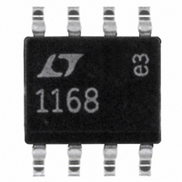
LT1168CS8#PBF Linear Technology, LT1168CS8#PBF Datasheet

LT1168CS8#PBF
Specifications of LT1168CS8#PBF
Available stocks
Related parts for LT1168CS8#PBF
LT1168CS8#PBF Summary of contents
Page 1
... SO packages, requires significantly less PC board area than discrete op amp resistor designs. These advantages make the LT1168 the most cost effective solution for precision instrumentation amplifier applications. , LT, LTC and LTM are registered trademarks of Linear Technology Corporation. All other trademarks are the property of their respective owners. 40k REF ...
Page 2
LT1168 ABSOLUTE AXI U RATI GS (Note 1) Supply Voltage ...................................................... ±20V Differential Input Voltage (Within the Supply Voltage) ..................................................... ±40V Input Voltage (Equal to Supply Voltage) ................ ±20V Input Current (Note 2) ....................................... ±20mA Output Short-Circuit ...
Page 3
ELECTRICAL CHARACTERISTICS SYMBOL PARAMETER C Differential Input Capacitance IN(DIFF) C Common Mode Input IN(CM) Capacitance V Input Voltage Range CM CMRR Common Mode Rejection Ratio PSRR Power Supply Rejection Ratio I Supply Current S V Output Voltage Swing OUT I ...
Page 4
LT1168 ELECTRICAL CHARACTERISTICS = ±15V, V temperature range 0V SYMBOL PARAMETER CONDITIONS (Note 6) V Total Input Referred Offset Voltage OST V Input Offset Voltage V OSI V Input Offset Voltage Hysteresis (Notes 7, 10) ...
Page 5
ELECTRICAL CHARACTERISTICS = ±15V, V temperature range 0V SYMBOL PARAMETER V Total Input Referred Offset Voltage OST V Input Offset Voltage OSI V Input Offset Voltage Hysteresis OSIH V Output Offset Voltage OSO V Output ...
Page 6
LT1168 W U TYPICAL PERFOR A CE CHARACTERISTICS Distribution of Output Offset Voltage 60 = ±15V V 299 N8 (2 LOTS 25°C 337 S0-8 (2 LOTS 636 TOTAL PARTS 45 40 ...
Page 7
W U TYPICAL PERFOR A CE CHARACTERISTICS 0.1Hz to 10Hz Noise Voltage ±15V 25° TIME (SEC) 1168 G10 0.1Hz to ...
Page 8
LT1168 W U TYPICAL PERFOR A CE CHARACTERISTICS Change in Input Bias Current for V = 20V ±15V V 302 N8 (2 LOTS ±10V 18 V 313 SO-8 (2 LOTS 25°C 615 ...
Page 9
W U TYPICAL PERFOR A CE CHARACTERISTICS Output Voltage Swing vs Load Current + ± 15V – 0 – 1 – 1 – 2.0 ...
Page 10
LT1168 W U TYPICAL PERFOR A CE CHARACTERISTICS Small-Signal Transient Response 1168 G34 10µs/DIV ±15V 60pF L Large-Signal Transient Response 1168 G37 G = 1000 200µs/DIV = ±15V ...
Page 11
W BLOCK DIAGRA + 400Ω –IN 2 – 400Ω +IN 3 –V S THEORY OF OPERATIO The LT1168 is a modified version of the three op amp instrumentation ...
Page 12
LT1168 THEORY OF OPERATIO voltage (R1 + R2)/ the unity-gain difference G amplifier A3. The common mode voltage is removed by A3, resulting in a single-ended output voltage referenced to the voltage on the REF pin. ...
Page 13
THEORY OF OPERATIO + AREA OF OPERATION –1 –2 – 100 –4 AREA OF OPERATION –5 – 25°C A INPUT COMMON –7 MODE RANGE IS BELOW THE CURVE – ...
Page 14
LT1168 THEORY OF OPERATIO path. The first example purely differential signal source with a 10kΩ input current path to ground. Since the impedance of the signal source is low, only one resistor is needed. Two matching resistors ...
Page 15
U U APPLICATIO S I FOR ATIO voltages or high levels of noise. Typically, the sources of these very small signals (on the order of microvolts or millivolts) are sensors that can be a significant distance from the signal conditioning ...
Page 16
LT1168 U U APPLICATIO S I FOR ATIO a ground for the common mode signal. C1 was chosen to maintain the stability of the patient ground. The LT1168’s high CMRR ensures that the desired differential signal is amplified and unwanted ...
Page 17
U TYPICAL APPLICATIO S R5 200k LT1490 2 LT1634CCZ-1.25 – 50k R3 50k R8 100k –IN +IN Single Supply Barometer V S LUCAS NOVA SENOR NPC-1220-015-A- – ...
Page 18
LT1168 U TYPICAL APPLICATIO 392k 1/4 2 LT1114 LT1634CCZ-1.25 2 – 0.6% ACCURACY AT ROOM TEMP 1.7% ACCURACY AT 0°C TO 60°C VOLTS INCHES Hg 2.800 28.00 3.000 30.00 3.200 32.00 18 ...
Page 19
... MOLD FLASH OR PROTRUSIONS SHALL NOT EXCEED .006" (0.15mm) Information furnished by Linear Technology Corporation is believed to be accurate and reliable. However, no responsibility is assumed for its use. Linear Technology Corporation makes no represen- tation that the interconnection of its circuits as described herein will not infringe on existing patent rights. ...
Page 20
... LT1462 6 – 1168 TA05 COMMENTS Switched Capacitor, Rail-to-Rail Input, 120dB CMRR 100 10µ 50pA 100 105µ 100, Slew Rate = 30V/µs Lower Noise than LT1168 7.5nV/√Hz N LT/LWI 0906 REV A • PRINTED IN USA © LINEAR TECHNOLOGY CORPORATION 2000 1168fa ...


