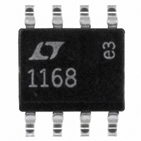
LT1168CS8#PBF Linear Technology, LT1168CS8#PBF Datasheet - Page 12

LT1168CS8#PBF
Manufacturer Part Number
LT1168CS8#PBF
Description
IC AMP INSTR PREC PROG 8-SOIC
Manufacturer
Linear Technology
Type
Instrumentation Ampr
Specifications of LT1168CS8#PBF
Amplifier Type
Instrumentation
Number Of Circuits
1
Slew Rate
0.5 V/µs
Gain Bandwidth Product
400kHz
Current - Input Bias
80pA
Voltage - Input Offset
20µV
Current - Supply
350µA
Current - Output / Channel
32mA
Voltage - Supply, Single/dual (±)
4.6 V ~ 36 V, ±2.3 V ~ 18 V
Operating Temperature
0°C ~ 70°C
Mounting Type
Surface Mount
Package / Case
8-SOIC (3.9mm Width)
Number Of Channels
1
Number Of Elements
1
Power Supply Requirement
Dual
Common Mode Rejection Ratio
85dB
Input Resistance
1250000@±15VMohm
Input Offset Voltage
0.06@±15VmV
Input Bias Current
0.0005@±15VnA
Single Supply Voltage (typ)
Not RequiredV
Dual Supply Voltage (typ)
15V
Power Supply Rejection Ratio
100dB
Rail/rail I/o Type
No
Single Supply Voltage (min)
Not RequiredV
Single Supply Voltage (max)
Not RequiredV
Dual Supply Voltage (min)
±2.3V
Dual Supply Voltage (max)
±18V
Operating Temp Range
0C to 70C
Operating Temperature Classification
Commercial
Mounting
Surface Mount
Pin Count
8
Package Type
SOIC N
Lead Free Status / RoHS Status
Lead free / RoHS Compliant
Output Type
-
-3db Bandwidth
-
Lead Free Status / Rohs Status
Compliant
Available stocks
Company
Part Number
Manufacturer
Quantity
Price
THEORY OF OPERATIO
LT1168
voltage, G = (R1 + R2)/R
amplifier A3. The common mode voltage is removed by
A3, resulting in a single-ended output voltage referenced
to the voltage on the REF pin. The resulting gain equation
is:
solving for the gain set resistor gives:
Table 1 shows appropriate 1% resistor values for a variety
of gains.
Table 1
DESIRED GAIN
1
2
5
10
20
50
100
200
500
1000
Input and Output Offset Voltage
The offset voltage of the LT1168 has two components: the
output offset and the input offset. The total offset voltage
referred to the input (RTI) is found by dividing the output
offset by the programmed gain (G) and adding it to the
input offset. At high gains the input offset voltage domi-
nates, whereas at low gains the output offset voltage
dominates. The total offset voltage is:
Reference Terminal
The reference terminal is one end of one of the four 30k
resistors around the difference amplifier. The output
12
G = (49.4kΩ / R
R
Total input offset voltage (RTI)
= input offset + (output offset/G)
Total output offset voltage (RTO)
= (input offset • G) + output offset
G
= 49.4kΩ /(G – 1)
5488.89Ω
1008.16Ω
498.99Ω
248.24Ω
49400Ω
12350Ω
49.95Ω
2600Ω
Open
99Ω
R
G
G
) + 1
CLOSEST 1% VALUE
G
, to the unity-gain difference
49900Ω
12400Ω
5490Ω
2610Ω
1000Ω
49.4Ω
499Ω
249Ω
100Ω
Open
U
RESULTANT GAIN
99.998
4.984
9.998
19.93
199.4
1001
1.99
50.4
495
1
voltage of the LT1168 (Pin 6) is referenced to the voltage
on the reference terminal (Pin 5). Resistance in series
with the REF pin must be minimized for best common
mode rejection. For example, a 6Ω resistance from the
REF pin to ground will not only increase the gain error by
0.02% but will lower the CMRR to 80dB.
Input Voltage Range
The input voltage range for the LT1168 is specified in the
data sheet at 1.4V below the positive supply to 1.9V
above the negative supply for a gain of one. As the gain
increases the input voltage range decreases. This is due
to the IR drop across the internal gain resistors R1 and
R2 in Figure 1. For the unity gain condition there is no IR
drop across the gain resistors R1 and R2, the output of
the GM amplifiers is just the differential input voltage at
Pin 2 and Pin 3 (level shifted by one V
When a gain resistor is connected across Pins 1 and 8,
the output swing of the GM cells is now the differential
input voltage (level shifted by V
voltage times the gain (ratio of the internal gain resistors
to the external gain resistor across Pins 1 and 8). To
calculate how close to the positive rail the input (V
swing for a gain of 2 and a maximum expected output
swing of 10V, use the following equation:
Substituting yields:
below the positive supply or 12V for a 15V supply. To
calculate how far above the negative supply the input can
swing for a gain of 10 with a maximum expected output
swing of –10V, the equation for the negative case is:
Substituting yields:
above the negative supply or – 9V for a negative supply
voltage of –15V. Figures 2 and 3 are for the positive
common mode and negative common mode cases
respectively.
+ V
– 0.5 – (10/2) • (1/2) = – 3V
– V
1.5 – (–10/10) • 9/2 = 6V
S
S
– V
+ V
IN
IN
= – 0.5 – (V
= 1.5 – (V
OUT
OUT
/G) • (G – 1)/2
/G) • (G – 1)/2
BE
) plus the differential
BE
from Q1 and Q2).
IN
) can
1168fa


