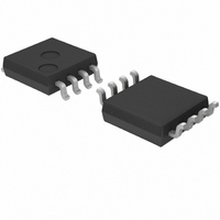
BU7442SFVM-TR Rohm Semiconductor, BU7442SFVM-TR Datasheet - Page 5

BU7442SFVM-TR
Manufacturer Part Number
BU7442SFVM-TR
Description
IC OPAMP 1.7-5.5V GRD SENS 8MSOP
Manufacturer
Rohm Semiconductor
Datasheet
1.BU7461G-TR.pdf
(37 pages)
Specifications of BU7442SFVM-TR
Amplifier Type
General Purpose
Number Of Circuits
2
Slew Rate
0.3 V/µs
Gain Bandwidth Product
600kHz
Current - Input Bias
1pA
Voltage - Input Offset
1000µV
Current - Supply
100µA
Current - Output / Channel
10mA
Voltage - Supply, Single/dual (±)
1.7 V ~ 5.5 V
Operating Temperature
-40°C ~ 105°C
Mounting Type
Surface Mount
Package / Case
8-MSOP, Micro8™, 8-uMAX, 8-uSOP,
Number Of Channels
2
Common Mode Rejection Ratio (min)
45 dB
Input Offset Voltage
6 mV
Input Bias Current (max)
1 pA
Output Current (typ)
6 mA, 10 mA
Operating Supply Voltage
1.7 V to 5.5 V
Supply Current
0.24 mA
Maximum Power Dissipation
480 mW
Maximum Operating Temperature
+ 105 C
Minimum Operating Temperature
- 40 C
Maximum Dual Supply Voltage
+/- 2.75 V
Minimum Dual Supply Voltage
+/- 0.85 V
Mounting Style
SMD/SMT
Shutdown
No
Supply Voltage (max)
5.5 V
Supply Voltage (min)
1.7 V
Technology
CMOS
Voltage Gain Db
95 dB
Lead Free Status / RoHS Status
Lead free / RoHS Compliant
Output Type
-
-3db Bandwidth
-
Lead Free Status / Rohs Status
Lead free / RoHS Compliant
Available stocks
Company
Part Number
Manufacturer
Quantity
Price
Company:
Part Number:
BU7442SFVM-TR
Manufacturer:
Rohm
Quantity:
5 186
BU7261/BU7261S family, BU7241/BU7241S family, BU7295/BU7295S family, BU7275/BU7275S family
BU7262/BU7262S family, BU7242/BU7242S family, BU7264/BU7264S family, BU7244/BU7244S family
© 2010 ROHM Co., Ltd. All rights reserved.
www.rohm.com
○BU7264 family (Unless otherwise specified VDD=+3[V], VSS=0[V], Ta=25[℃])
Input Offset Voltage
Input Offset Current
Input Bias Current
Supply Current
High Level Output Voltage
Low Level Output Voltage
Large Signal Voltage Gain
Input Common-mode Voltage Range
Common-mode Rejection Ratio
Power Supply Rejection Ratio
Output Source Current
Output Sink Current
Slew Rate
Gain Band width
Phase Margin
Total Harmonic Distortion
Channel Separation
(*8)
(*9)
(*10) Under the high temperature environment, consider the power dissipation of IC when selecting the output current.
Absolute value
Full range: BU7264: Ta=-40[℃] ~ +85[℃] BU7264S: Ta=-40[℃] ~ +105[℃]
When the terminal short circuits are continuously output, the output current is reduced to climb to the temperature inside IC.
Parameter
(*9)
(*8)
(*8)(*9)
(*8)
(*10)
(*10)
Symbol
CMRR
PSRR
VOH
Vicm
VOL
THD
IOH
IDD
IOL
Vio
SR
CS
AV
FT
Iio
Ib
θ
Temperature
Full range
Full range
Range
25℃
25℃
25℃
25℃
25℃
25℃
25℃
25℃
25℃
25℃
25℃
25℃
25℃
25℃
25℃
25℃
25℃
5/36
VDD-0.1
Min.
70
45
60
-
-
-
-
-
-
-
-
-
-
-
-
0
4
5
BU7264SF
BU7264F
Limits
1100
Typ.
0.05
100
1.1
95
60
80
10
12
50
-
-
-
-
1
1
1
2
-
VSS+0.1
Max.
2300
2800
10
-
-
-
-
-
-
-
-
-
-
-
-
-
9
3
V/μs CL=25[pF]
MHz CL=25[pF], AV=40[dB]
Unit
mV
mA
mA
pA
pA
μA
dB
dB
dB
dB
%
V
V
V
°
VDD=1.8 ~ 5.5[V]
VOUT=VDD/2
RL=∞ All Op-Amps
AV=0[dB], VIN=1.5[V]
RL=10[kΩ]
RL=10[kΩ]
RL=10[kΩ]
VDD-VSS=3[V]
VDD-0.4[V]
VSS+0.4[V]
CL=25[pF], AV=40[dB]
VOUT=0.8[Vp-p],
f=1[kHz]
AV=40[dB]
Technical Note
2010.12 - Rev.A
Condition
-
-
-
-


