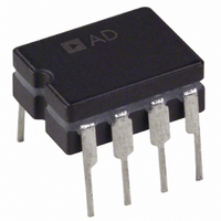
OP270EZ Analog Devices Inc, OP270EZ Datasheet - Page 17

OP270EZ
Manufacturer Part Number
OP270EZ
Description
IC OPAMP GP 5MHZ DUAL PREC 8CDIP
Manufacturer
Analog Devices Inc
Specifications of OP270EZ
Slew Rate
2.4 V/µs
Rohs Status
RoHS non-compliant
Amplifier Type
General Purpose
Number Of Circuits
2
Gain Bandwidth Product
5MHz
Current - Input Bias
5nA
Voltage - Input Offset
10µV
Current - Supply
4mA
Voltage - Supply, Single/dual (±)
±4.5 V ~ 18 V
Operating Temperature
-40°C ~ 85°C
Mounting Type
Through Hole
Package / Case
8-CDIP (0.300", 7.62mm)
Op Amp Type
Low Noise
No. Of Amplifiers
2
Bandwidth
5MHz
Supply Voltage Range
± 4.5V To ± 18V
Amplifier Case Style
DIP
No. Of Pins
8
Channel Separation
175
Common Mode Rejection Ratio
125
Current, Input Bias
5 nA
Current, Input Offset
1 nA
Current, Supply
4 mA
Impedance, Thermal
12 °C/W
Number Of Amplifiers
Dual
Package Type
CDIP-8
Resistance, Input
0.4 Megohms (Differential), 20 Gigaohms (Common-Mode)
Temperature, Operating, Range
-40 to +85 °C
Voltage, Gain
2300 V/mV
Voltage, Input
±12.5 V
Voltage, Noise
3.6 nV/sqrt Hz
Voltage, Offset
10 μV
Voltage, Output, High
+13.5 V
Voltage, Output, Low
-13.5 V
Voltage, Supply
±15 V
Output Type
-
Current - Output / Channel
-
-3db Bandwidth
-
Lead Free Status / RoHS Status
Contains lead / RoHS non-compliant
Available stocks
Company
Part Number
Manufacturer
Quantity
Price
Company:
Part Number:
OP270EZ
Manufacturer:
PMI
Quantity:
5 510
Company:
Part Number:
OP270EZ/FZ
Manufacturer:
PMI
Quantity:
5 510
Company:
Part Number:
OP270EZ/FZ
Manufacturer:
NAIS
Quantity:
5 510
DIGITAL PANNING CONTROL
Figure 44 uses a
signal between two channels. One channel is formed by the
current output of DAC A driving one-half of an OP270 in a
current-to-voltage converter configuration. The other channel
is formed by the complementary output current of DAC A,
which normally flows to ground through the AGND pin. This
complementary current is converted to a voltage by the other
half of the OP270, which also holds AGND at virtual ground.
Gain error due to mismatching between the internal DAC
ladder resistors and the current-to-voltage feedback resistors is
eliminated by using feedback resistors internal to the DAC8221.
Only DAC A passes a signal; DAC B provides the second
feedback resistor. With V
voltage converter, using R
digital data reaching DAC B. Distortion of the digital panning
control is less than 0.002% over the 20 Hz to 20 kHz audio
range. Figure 45 shows the complementary outputs for a 1 kHz
input signal and a digital ramp applied to the DAC data input.
DUAL PROGRAMMABLE GAIN AMPLIFIER
The dual OP270 and the DAC8221 (a dual 12-bit CMOS DAC)
can be combined to form a space-saving, dual programmable
amplifier. The digital code present at the DAC, which is easily
set by a microprocessor, determines the ratio between the internal
feedback resistor and the resistance that the DAC ladder presents
to the op amp feedback loop. Gain of each amplifier is
where n is the decimal equivalent of the 12-bit digital code
present at the DAC.
If the digital code present at the DAC consists of all 0s, the
feedback loop opens, causing the op amp output to saturate. A
20 MΩ resistor placed in parallel with the DAC feedback loop
eliminates this problem with only a very small reduction in gain
accuracy.
V
V
IN
O
=
−
4096
n
DAC8221
REF
FBB
(a dual 12-bit CMOS DAC) to pan a
B unconnected, the current-to-
, is accurate and not influenced by
Rev. E | Page 17 of 20
CONTROL
WRITE
A OUT
A OUT
PINS 6 (MSB) TO 17 (LSB)
V
NC
IN
DAC DATA BUS
22
18
19
20
4
V
V
DAC A/DAC B
CS
WR
DAC8221P
REF
REF
5V
Figure 45. Digital Panning Control Output
A
B
Figure 44. Digital Panning Control
5V
DAC A
DAC B
DGND
+5V
V
DD
21
5
AGND
I
I
R
R
OUT
OUT
FBA
FBB
A
B
23
24
3
2
1
2
3
6
5
OP270GP
OP270GP
+15V
–15V
1/2
1/2
8
4
1ms
+
–
1
7
0.01µF
10µF
0.1µF
OP270
+
–
10µF
OUT
OUT


