AD549LHZ Analog Devices Inc, AD549LHZ Datasheet - Page 10
AD549LHZ
Manufacturer Part Number
AD549LHZ
Description
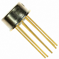
IC OPAMP GP 1MHZ LP 20MA TO99-8
Manufacturer
Analog Devices Inc
Series
Topgate™r
Datasheet
1.AD549JHZ.pdf
(20 pages)
Specifications of AD549LHZ
Slew Rate
3 V/µs
Amplifier Type
General Purpose
Number Of Circuits
1
Gain Bandwidth Product
1MHz
Current - Input Bias
0.04pA
Voltage - Input Offset
300µV
Current - Supply
600µA
Current - Output / Channel
20mA
Voltage - Supply, Single/dual (±)
±5 V ~ 18 V
Operating Temperature
0°C ~ 70°C
Mounting Type
Through Hole
Package / Case
TO-99-8, Metal Can
Op Amp Type
Low Bias Current
No. Of Amplifiers
1
Bandwidth
1MHz
Supply Voltage Range
± 5V To ± 18V
Amplifier Case Style
TO-99
No. Of Pins
8
Lead Free Status / RoHS Status
Lead free / RoHS Compliant
Output Type
-
-3db Bandwidth
-
Lead Free Status / Rohs Status
RoHS Compliant part
Electrostatic Device
Available stocks
Company
Part Number
Manufacturer
Quantity
Price

Part Number:
AD549LHZ
Manufacturer:
ADI/亚德诺
Quantity:
20 000


AD549
FUNCTIONAL DESCRIPTION
MINIMIZING INPUT CURRENT
The AD549 is optimized for low input current and offset
voltage. Careful attention to how the amplifier is used reduces
input currents in actual applications.
Keep the amplifier operating temperature as low as possible to
minimize input current. Like other JFET input amplifiers, the
AD549 input current is sensitive to chip temperature, rising by
a factor of 2.3 for every 10°C. Figure 25 is a plot of the AD549
input current vs. ambient temperature.
On-chip power dissipation raises the chip operating tempera-
ture, causing an increase in input bias current. Due to the low
quiescent supply current of the AD549, the chip temperature
is less than 3°C higher than its ambient temperature when the
(unloaded) amplifier is operating with 15 V supplies. The
difference in the input current is negligible.
However, heavy output loads can cause a significant increase in
chip temperature and a corresponding increase in the input
current. Maintaining a minimum load resistance of 10 Ω is
recommended. Input current vs. additional power dissipation
due to output drive current is plotted in Figure 26.
100pA
100fA
10pA
Figure 26. Input Bias Current vs. Additional Power Dissipation
10fA
1nA
1pA
1fA
6
5
4
3
2
1
Figure 25. Input Bias Current vs. Ambient Temperature
–55
0
ADDITIONAL INTERNAL POWER DISSIPATION (mW)
25
–25
50
5
TEMPERATURE (°C)
75
BASED ON
TYPICAL I
100
35
B
125
= 40fA
65
150
95
175
200
125
Rev. H | Page 10 of 20
CIRCUIT BOARD NOTES
A number of physical phenomena generate spurious currents
that degrade the accuracy of low current measurements. Figure 27
is a schematic of a current to voltage (I-to-V) converter with
these parasitic currents modeled.
Finite resistance from input lines to voltages on the board,
modeled by Resistor R
resistance of more than 10
the amplifier signal and supply lines to capitalize on the low
input currents of the AD549. Standard PCB material does not
have high enough insulation resistance; therefore, connect the
input leads of the AD549 to standoffs made of insulating
material with adequate volume resistivity (that is, Teflon®). The
surface of the insulator must be kept clean to preserve surface
resistivity. For Teflon, an effective cleaning procedure consists
of swabbing the surface with high grade isopropyl alcohol,
rinsing with deionized water, and baking the board at 80°C for
10 minutes.
In addition to high volume and surface resistivity, other proper-
ties are desirable in the insulating material chosen. Resistance
to water absorption is important because surface water films
drastically reduce surface resistivity. The insulator chosen
should also exhibit minimal piezoelectric effects (charge
emission due to mechanical stress) and triboelectric effects
(charge generated by friction). Charge imbalances generated
by these mechanisms can appear as parasitic leakage currents.
These effects are modeled by Variable Capacitor C
Table 3 lists various insulators and their properties.
Guarding the input lines by completely surrounding them with
a metal conductor biased near the potential of the input lines
has two major benefits. First, parasitic leakage from the signal
line is reduced because the voltage between the input line and
the guard is very low. Second, stray capacitance at the input
node is minimized. Input capacitance can substantially degrade
signal bandwidth and the stability of the I-to-V converter.
1
Electronic Measurements, pp. 15–17, Keithley Instruments, Inc., Cleveland,
Ohio, 1977.
Figure 27. Sources of Parasitic Leakage Currents
V
R
S
P
f
S
P
, results in parasitic leakage. Insulation
C
15
P
Ω must be maintained between
2
3
I
I'
AD549
=
R
V
P
+
8
dC
dT
C
R
P
F
F
V +
6
dV
dT
C
P
V
P
OUT
in Figure 27.
+
–
1
Related parts for AD549LHZ
Image
Part Number
Description
Manufacturer
Datasheet
Request
R

Part Number:
Description:
±1.7g Dual-Axis IMEMS Accelerometer Evaluation Board
Manufacturer:
Analog Devices Inc
Datasheet:

Part Number:
Description:
Inertial Sensor Evaluation System
Manufacturer:
Analog Devices Inc
Datasheet:
Part Number:
Description:
Manufacturer:
Analog Devices Inc
Datasheet:
Part Number:
Description:
Manufacturer:
Analog Devices Inc
Datasheet:
Part Number:
Description:
Manufacturer:
Analog Devices Inc
Datasheet:
Part Number:
Description:
Manufacturer:
Analog Devices Inc
Datasheet:
Part Number:
Description:
Manufacturer:
Analog Devices Inc
Datasheet:
Part Number:
Description:
Manufacturer:
Analog Devices Inc
Datasheet:
Part Number:
Description:
Manufacturer:
Analog Devices Inc
Datasheet:
Part Number:
Description:
Manufacturer:
Analog Devices Inc
Datasheet:
Part Number:
Description:
Manufacturer:
Analog Devices Inc
Datasheet:
Part Number:
Description:
Manufacturer:
Analog Devices Inc
Datasheet:
Part Number:
Description:
Manufacturer:
Analog Devices Inc
Datasheet: