AD549LHZ Analog Devices Inc, AD549LHZ Datasheet - Page 15
AD549LHZ
Manufacturer Part Number
AD549LHZ
Description
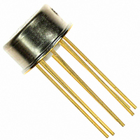
IC OPAMP GP 1MHZ LP 20MA TO99-8
Manufacturer
Analog Devices Inc
Series
Topgate™r
Datasheet
1.AD549JHZ.pdf
(20 pages)
Specifications of AD549LHZ
Slew Rate
3 V/µs
Amplifier Type
General Purpose
Number Of Circuits
1
Gain Bandwidth Product
1MHz
Current - Input Bias
0.04pA
Voltage - Input Offset
300µV
Current - Supply
600µA
Current - Output / Channel
20mA
Voltage - Supply, Single/dual (±)
±5 V ~ 18 V
Operating Temperature
0°C ~ 70°C
Mounting Type
Through Hole
Package / Case
TO-99-8, Metal Can
Op Amp Type
Low Bias Current
No. Of Amplifiers
1
Bandwidth
1MHz
Supply Voltage Range
± 5V To ± 18V
Amplifier Case Style
TO-99
No. Of Pins
8
Lead Free Status / RoHS Status
Lead free / RoHS Compliant
Output Type
-
-3db Bandwidth
-
Lead Free Status / Rohs Status
RoHS Compliant part
Electrostatic Device
Available stocks
Company
Part Number
Manufacturer
Quantity
Price

Part Number:
AD549LHZ
Manufacturer:
ADI/亚德诺
Quantity:
20 000


Input current, I
proportional to the feedback resistance
The input voltage offset of the op amp causes an error current
through the photodiode shunt resistance, R
The error current results in an error voltage (V
amplifier output equal to
Given typical values of photodiode shunt resistance (on the order
of 10
feedback resistance is used. Also, R
ture because photodiode shunt resistance typically drops by a
factor of 2 for every 10°C rise in temperature. An op amp with
low offset voltage and low drift must be used to maintain accuracy.
The AD549K offers a guaranteed maximum 0.25 mV offset
voltage and 5 mV/°C drift for very sensitive applications.
Photodiode Preamp Noise
Noise limits the signal resolution obtainable with the preamp.
The output voltage noise divided by the feedback resistance is
the minimum current signal that can be detected. This mini-
mum detectable current divided by the responsivity of the
photodiode represents the lowest light power that is detectable
by the preamp.
Noise sources associated with the photodiode, amplifier, and
feedback resistance are shown in Figure 43; Figure 44 is the
spectral density vs. frequency plot of the contribution of each of
the noise sources to the output voltage noise (circuit parameters
in Figure 42 are assumed). The rms contribution of each noise
source to the total output voltage noise is obtained by
integrating the square of its spectral density function over
frequency. The rms value of the output voltage noise is the
square root of the sum of all contributions. Minimizing the total
area under these curves optimizes the resolution of the
preamplifier for a given bandwidth.
The photodiode preamp in Figure 41 can detect a signal current
of 26 fA rms at a bandwidth of 16 Hz, which, assuming a
photodiode responsivity of 0.5 A/W, translates to a 52 fW rms
minimum detectable power. The photodiode used has a high
source resistance and low junction capacitance. C
signal bandwidth with R
V
I = V
V
9
I
S
Ω), R
E1
E2
= I
= (1 + R
OS
B
/R
F
/R
R
× R
Figure 43. Photodiode Preamp Noise Sources
S
S
S
B
can easily be greater than 1, especially if a large
, contributes an output voltage error, V
F
F
/R
C
S
)V
S
OS
F
and also limits the peak in the noise
IN
R
IF
EN
F
F
/R
S
increases with tempera-
S
A
E2
) at the
C
F
F
sets the
E1
,
Rev. H | Page 15 of 20
gain that multiplies the op amp input voltage noise contribu-
tion. A single-pole filter at the output of the amplifier limits the
op amp output voltage noise bandwidth to 26 Hz, comparable
to the signal bandwidth. This greatly improves the signal-to-
noise ratio of the preamplifier (in this case, by a factor of 3).
LOG RATIO AMPLIFIER
Logarithmic ratio circuits are useful for processing signals with
wide dynamic range. The 60 fA maximum input current of the
AD549L makes it possible to build a log ratio amplifier with
1% log conformance for input currents ranging from 10 pA to
1 mA, a dynamic range of 160 dB.
The log ratio amplifier in Figure 45 provides an output voltage
proportional to the log base 10 of the ratio of Input Current I
and Input Current I
for voltage inputs. Because NPN devices are used in the feedback
loop of the front-end amplifiers that provide the log transfer
function, the output is valid only for positive input voltages and
input currents. The input currents set the Collector Current IC1
and Collector Current IC2 of a matched pair of log transistors,
Q1 and Q2, to develop Voltage V
where IES is the saturation current of the transistor.
The difference of V
obtain
V
approximately 16 at room temperature, resulting in the output
voltage
R8 is a resistor with a positive 3500 ppm/°C temperature coeffi-
cient to provide the necessary temperature compensation. The
parallel combination of R15 and R7 is provided to keep the gain
of the subtractor section for positive and negative inputs matched
over temperature.
C
is scaled up by the ratio of (R9 + R10)/R8, which is equal to
V
V
V
A
C
OUT
100n
Figure 44. Spectral Density of the Photodiode Preamp Noise
, V
10n
10µ
= (kT/q)ln(IC2/IC1)
1µ
= 1 V × log(IC2/IC1)
B
1
= –(kT/q)ln IC/IES
EN
CONTRIBUTION,
WITH FILTER
10
A
2
. Resistor R1 and Resistor R2 are provided
and V
IF AND CS, NO FILTERS
Sources vs. Frequency
100
IF AND CS, WITH FILTERS
B
FREQUENCY (Hz)
is taken by the subtractor section to
OPEN-LOOP GAIN
A
1k
and Voltage V
AD549
EN CONTRIBUTION,
NO FILTER
10k
B
100k
AD549
1M
1
Related parts for AD549LHZ
Image
Part Number
Description
Manufacturer
Datasheet
Request
R

Part Number:
Description:
±1.7g Dual-Axis IMEMS Accelerometer Evaluation Board
Manufacturer:
Analog Devices Inc
Datasheet:

Part Number:
Description:
Inertial Sensor Evaluation System
Manufacturer:
Analog Devices Inc
Datasheet:
Part Number:
Description:
Manufacturer:
Analog Devices Inc
Datasheet:
Part Number:
Description:
Manufacturer:
Analog Devices Inc
Datasheet:
Part Number:
Description:
Manufacturer:
Analog Devices Inc
Datasheet:
Part Number:
Description:
Manufacturer:
Analog Devices Inc
Datasheet:
Part Number:
Description:
Manufacturer:
Analog Devices Inc
Datasheet:
Part Number:
Description:
Manufacturer:
Analog Devices Inc
Datasheet:
Part Number:
Description:
Manufacturer:
Analog Devices Inc
Datasheet:
Part Number:
Description:
Manufacturer:
Analog Devices Inc
Datasheet:
Part Number:
Description:
Manufacturer:
Analog Devices Inc
Datasheet:
Part Number:
Description:
Manufacturer:
Analog Devices Inc
Datasheet:
Part Number:
Description:
Manufacturer:
Analog Devices Inc
Datasheet: