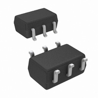
LMH6601QMG/NOPB National Semiconductor, LMH6601QMG/NOPB Datasheet - Page 17

LMH6601QMG/NOPB
Manufacturer Part Number
LMH6601QMG/NOPB
Description
IC AMP VFA 2.4V SHUTDOWN SC70-6
Manufacturer
National Semiconductor
Datasheet
1.LMH6601MGNOPB.pdf
(28 pages)
Specifications of LMH6601QMG/NOPB
Amplifier Type
Voltage Feedback
Number Of Circuits
1
Output Type
Rail-to-Rail
Slew Rate
275 V/µs
Gain Bandwidth Product
155MHz
-3db Bandwidth
250MHz
Current - Input Bias
5pA
Voltage - Input Offset
1000µV
Current - Supply
9.6mA
Current - Output / Channel
180mA
Voltage - Supply, Single/dual (±)
2.4 V ~ 5.5 V, ±1.2 V ~ 2.75 V
Operating Temperature
-40°C ~ 85°C
Mounting Type
Surface Mount
Package / Case
SC-70-6, SC-88, SOT-363
Number Of Channels
1
Voltage Gain Db
66 dB
Common Mode Rejection Ratio (min)
56 dB
Input Offset Voltage
2.4 mV at 5 V
Operating Supply Voltage
3 V, 5 V
Supply Current
11.5 mA at 5 V
Maximum Operating Temperature
+ 85 C
Minimum Operating Temperature
- 40 C
Lead Free Status / RoHS Status
Lead free / RoHS Compliant
Other names
LMH6601QMG
LMH6601QMG
LMH6601QMGTR
LMH6601QMG
LMH6601QMGTR
Available stocks
Company
Part Number
Manufacturer
Quantity
Price
Company:
Part Number:
LMH6601QMG/NOPB
Manufacturer:
National Semiconductor
Quantity:
1 976
Application Information
OPTIMIZING PERFORMANCE
With many op amps, additional device non-linearity and
sometimes less loop stability arises when the output has to
switch from current-source mode to current-sink mode or vice
versa. When it comes to achieving the lowest distortion and
the best Differential Gain/ Differential Phase (DG/ DP, broad-
cast video specs), the LMH6601 is optimized for single supply
DC coupled output applications where the load current is re-
turned to the negative rail (V
is most linear (lowest distortion) and which corresponds to
unipolar current flowing out of this device. To that effect, it is
easy to see that the distortion specifications improve when
the output is only sourcing current which is the distortion-op-
timized mode of operation for the LMH6601. In application
where the LMH6601 output is AC coupled or when it is pow-
ered by separate dual supplies for V
supplies both source and sink current to the load and results
in less than optimum distortion (and DG/DP).
pares the distortion results between a DC and an AC coupled
load to show the magnitude of this difference. See the DG/DP
plots in the Typical Performance Characteristics section for a
comparison between DC and AC coupling of the video load.
In certain applications, it may be possible to optimize the
LMH6601 for best distortion (and DG/DP) even though the
load may require bipolar output current by adding a pull-down
resistor to the output. Adding an output pull-down resistance
of appropriate value could change the LMH6601 output load-
ing into source-only. This comes at the price of higher total
power dissipation and increased output current requirement.
Figure 2
for both the dual supply and for the AC coupled load applica-
tions.
FIGURE 1. Distortion Comparison between DC & AC
shows how to calculate the pull-down resistor value
Coupling of the Load
−
). That is where the output stage
+
and V
−
, the output stage
Figure 1
20136406
com-
17
FIGURE 2. Output Pull-Down Value for Dual Supply & AC
Furthermore, with a combination of low closed loop gain set-
ting (i.e. A
highest), light output loading (R
cant capacitive load (C
if output sink current is kept to less than about 5 mA. The pull-
down method described in
cases as well where the current that would normally be sunk
by the op amp is diverted to the R
SHUTDOWN CAPABILITY AND TURN ON/ OFF
BEHAVIOR
With the device in shutdown mode, the output goes into high
impedance (R
path between the inputs and the output pin is through the ex-
ternal components around the device. So, for applications
where there is active signal connection to the inverting input,
with the LMH6601 in shutdown, the output could show signal
swings due to current flow through these external compo-
nents. For non-inverting amplifiers in shutdown, no output
swings would occur, because of complete input-output isola-
tion, with the exception of capacitive coupling.
For maximum power saving, the LMH6601 supply current
drops to around 0.1 μA in shutdown. All significant power
consumption within the device is disabled for this purpose.
Because of this, the LMH6601 turn on time is measured in
micro-seconds whereas its turn off is fast (nano-seconds) as
would be expected from a high speed device like this.
The LMH6601 SD pin is a CMOS compatible input with a pico-
ampere range input current drive requirement. This pin needs
to be tied to a level or otherwise the device state would be
indeterminate. The device shutdown threshold is half way be-
tween the V
example, with V
expect the threshold to be at 7.5V. The state of the device
(shutdown or normal operation) is guaranteed over tempera-
ture as longs as the SD pin is held to within 10% of the total
supply voltage.
For V
•
•
Shutdown Range
Normal Operation Range
+
= 10V, V
V
+
= +1 for example where device bandwidth is the
and V
OUT
−
+
= 5V, as an example:
tied to 10V and V
> 100 MΩ) mode. In this mode, the only
−
pin potentials at any supply voltage. For
L
> 10 pF) , the LMH6601 is most stable
Coupling
Figure 2
L
> 1 kΩ) , and with a signifi-
P
path instead.
−
is applicable in these
equal to 5V, you can
9.5V
5V
≤
≤
www.national.com
SD
SD
≤
≤
20136470
5.5V
10V


