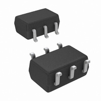
LMH6601QMG/NOPB National Semiconductor, LMH6601QMG/NOPB Datasheet - Page 25

LMH6601QMG/NOPB
Manufacturer Part Number
LMH6601QMG/NOPB
Description
IC AMP VFA 2.4V SHUTDOWN SC70-6
Manufacturer
National Semiconductor
Datasheet
1.LMH6601MGNOPB.pdf
(28 pages)
Specifications of LMH6601QMG/NOPB
Amplifier Type
Voltage Feedback
Number Of Circuits
1
Output Type
Rail-to-Rail
Slew Rate
275 V/µs
Gain Bandwidth Product
155MHz
-3db Bandwidth
250MHz
Current - Input Bias
5pA
Voltage - Input Offset
1000µV
Current - Supply
9.6mA
Current - Output / Channel
180mA
Voltage - Supply, Single/dual (±)
2.4 V ~ 5.5 V, ±1.2 V ~ 2.75 V
Operating Temperature
-40°C ~ 85°C
Mounting Type
Surface Mount
Package / Case
SC-70-6, SC-88, SOT-363
Number Of Channels
1
Voltage Gain Db
66 dB
Common Mode Rejection Ratio (min)
56 dB
Input Offset Voltage
2.4 mV at 5 V
Operating Supply Voltage
3 V, 5 V
Supply Current
11.5 mA at 5 V
Maximum Operating Temperature
+ 85 C
Minimum Operating Temperature
- 40 C
Lead Free Status / RoHS Status
Lead free / RoHS Compliant
Other names
LMH6601QMG
LMH6601QMG
LMH6601QMGTR
LMH6601QMG
LMH6601QMGTR
Available stocks
Company
Part Number
Manufacturer
Quantity
Price
Company:
Part Number:
LMH6601QMG/NOPB
Manufacturer:
National Semiconductor
Quantity:
1 976
TRANSIMPEDANCE AMPLIFIER NOISE
CONSIDERATIONS
When analyzing the noise at the output of the I-V converter,
it is important to note that the various noise sources (i.e. op
amp noise voltage, feedback resistor thermal noise, input
noise current, photodiode noise current) do not all operate
over the same frequency band. Therefore, when the noise at
the output is calculated, this should be taken into account.
The op amp noise voltage will be gained up in the region be-
tween the noise gain’s “zero” and its “pole” (f
14). The higher the values of R
gain peaking starts and therefore its contribution to the total
output noise would be larger. It is obvious to note that it is
advantageous to minimize C
amp, by applying a reverse bias across the diode at the ex-
pense of excess dark current and noise). However, most low
noise op amps have a higher input capacitance compared to
ordinary op amps. This is due to the low noise op amp’s larger
input stage.
OTHER APPLICATIONS
CAPACITIVE LOAD
The LMH6601 can drive a capacitive load of up to 1000 pF
with correct isolation and compensation.
the in-loop compensation technique to drive a large capacitive
load.
FIGURE 15. Charge Preamplifier Taking Advantage of
LMH6601’s Femto-Ampere Range Input Bias Current
IN
F
and C
(e.g. by proper choice of op
IN
, the sooner the noise
Figure 16
z
and f
p
illustrates
in
20136463
Figure
25
When driving a high capacitive load, an isolation resistor
(R
put and the capacitive load to provide isolation and to avoid
oscillations. A small value capacitor (C
the op amp output and the inverting input as shown such that
this capacitor becomes the dominant feedback path at higher
frequency. Together these components allow heavy capaci-
tive loading while keeping the loop stable.
There are few factors which affect the driving capability of the
op amp:
•
•
Table 4
of load capacitors (C
sistor (C
* Response limited by input step generator rise time of 5 ns
Figure 17
crease) at V
trade-off between the two:
FIGURE 16. In-Loop Compensation Circuit for Driving a
TABLE 4. LMH6601 Step Response Summary for the
S
Op amp internal architecture
Closed loop gain and output capacitor loading
) should be connected in series between the op amp out-
(pF)
110
300
500
910
C
10
50
L
shows the measured step response for various values
F
) with gain of +2 (R
shows the increase in rise/fall time (bandwidth de-
OUT
192
(Ω)
R
47
80
0
0
6
S
with larger capacitive loads, illustrating the
Heavy Capacitive Load
Circuit of
L
), series resistor (R
(pF)
C
10
10
10
1
1
1
F
F
= R
Figure 16
G
t
= 604Ω) and R
rise
(ns)
10
12
33
65
6*
7*
F
/ t
) is inserted between
fall
S
) and feedback re-
Overshoot
www.national.com
L
(%)
16
20
10
10
= 2 kΩ:
8
6
20136468


