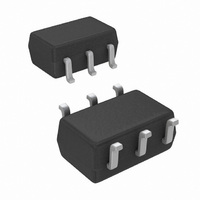
LMH6601QMG/NOPB National Semiconductor, LMH6601QMG/NOPB Datasheet - Page 24

LMH6601QMG/NOPB
Manufacturer Part Number
LMH6601QMG/NOPB
Description
IC AMP VFA 2.4V SHUTDOWN SC70-6
Manufacturer
National Semiconductor
Datasheet
1.LMH6601MGNOPB.pdf
(28 pages)
Specifications of LMH6601QMG/NOPB
Amplifier Type
Voltage Feedback
Number Of Circuits
1
Output Type
Rail-to-Rail
Slew Rate
275 V/µs
Gain Bandwidth Product
155MHz
-3db Bandwidth
250MHz
Current - Input Bias
5pA
Voltage - Input Offset
1000µV
Current - Supply
9.6mA
Current - Output / Channel
180mA
Voltage - Supply, Single/dual (±)
2.4 V ~ 5.5 V, ±1.2 V ~ 2.75 V
Operating Temperature
-40°C ~ 85°C
Mounting Type
Surface Mount
Package / Case
SC-70-6, SC-88, SOT-363
Number Of Channels
1
Voltage Gain Db
66 dB
Common Mode Rejection Ratio (min)
56 dB
Input Offset Voltage
2.4 mV at 5 V
Operating Supply Voltage
3 V, 5 V
Supply Current
11.5 mA at 5 V
Maximum Operating Temperature
+ 85 C
Minimum Operating Temperature
- 40 C
Lead Free Status / RoHS Status
Lead free / RoHS Compliant
Other names
LMH6601QMG
LMH6601QMG
LMH6601QMGTR
LMH6601QMG
LMH6601QMGTR
Available stocks
Company
Part Number
Manufacturer
Quantity
Price
Company:
Part Number:
LMH6601QMG/NOPB
Manufacturer:
National Semiconductor
Quantity:
1 976
www.national.com
The diode capacitance (C
of the LMH6601 (C
cuit and how it is compensated. With large transimpedance
gain values (R
plifier inverting input (C
create a zero in the Noise Gain (NG) function (see
14). If left untreated, at higher frequencies where NG equals
the open loop transfer function there will be excess phase shift
around the loop (approaching 180°) and therefore, the circuit
could be unstable. This is illustrated in
FIGURE 14. Transimpedance Amplifier Graphical
(pF)
500
C
10
50
D
Stability Analysis and Compensation
F
), the total combined capacitance on the am-
TABLE 3. Transimpedance Amplifier
(pF)
502
C
12
52
A
IN
) has a bearing on the stability of this cir-
GBWP = 155 MHz
IN
C
D
= C
V
) along with the input capacitance
A
S
= 2 pF
C
= 5V
D
F
+ C
_Calculated
(pF)
A
1.1
2.3
7.2
) will work against R
Figure
14.
C
Figure
20136460
F
(pF)
used
F
1
3
8
Figure 12
to
24
Compensation and Performance Results
Figure 14
value, across R
For optimum performance, this capacitor is usually picked so
that NG is equal to the op amp's open loop gain at f
cause a “flattening” of the NG slope beyond the point of in-
tercept of the two plots (open loop gain and NG) and will
results in a Phase Margin (PM) of 45° assuming f
at least a decade apart. This is because at the point of inter-
cept, the NG pole at f
which leaves 45° of PM. For reference,
the transimpedance gain (I-V (Ω))
Here is the theoretical expression for the optimum C
and the expected −3 dB bandwidth:
Table
and conditions, of testing the LMH6601 with various photodi-
odes having different capacitances (C
gain (R
Calculated (MHz)
−3 dB BW
3, below, lists the results, along with the assumptions
F
) of 10 kΩ.
14
7
2
shows that placing a capacitor, C
F
will create a pole in the NG function at f
P
Measured (MHz)
will have a 45° phase lead contribution
−3 dB BW
7.0
2.5
15
D
) at a transimpedance
Figure 14
Step Response
Overshoot (%)
F
, with the proper
P
also shows
6
4
9
P
and f
. This will
F
value
Z
(10)
are
(9)
P
.


