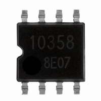
BA10358F-E2 Rohm Semiconductor, BA10358F-E2 Datasheet - Page 19

BA10358F-E2
Manufacturer Part Number
BA10358F-E2
Description
IC OPAMP DUAL 32V SOP8
Manufacturer
Rohm Semiconductor
Specifications of BA10358F-E2
Slew Rate
0.2 V/µs
Amplifier Type
General Purpose
Number Of Circuits
2
Gain Bandwidth Product
500kHz
Current - Input Bias
45nA
Voltage - Input Offset
2000µV
Current - Supply
700µA
Current - Output / Channel
20mA
Voltage - Supply, Single/dual (±)
3 V ~ 32 V, ±1.5 V ~ 16 V
Operating Temperature
-40°C ~ 85°C
Mounting Type
Surface Mount
Package / Case
8-SOP
Op Amp Type
General Purpose
No. Of Amplifiers
2
Bandwidth
1.2MHz
Supply Voltage Range
3V To 32V
Amplifier Case Style
SOIC
No. Of Pins
8
Operating Temperature Range
-40°C To +85°C
Number Of Channels
2
Voltage Gain Db
100 dB
Common Mode Rejection Ratio (min)
65 dB
Input Offset Voltage
7 mV
Operating Supply Voltage
3 V to 32 V
Supply Current
0.7 mA
Maximum Power Dissipation
550 mW
Maximum Operating Temperature
+ 85 C
Mounting Style
SMD/SMT
Maximum Dual Supply Voltage
+/- 16 V
Minimum Operating Temperature
- 40 C
Lead Free Status / RoHS Status
Lead free / RoHS Compliant
Output Type
-
-3db Bandwidth
-
Lead Free Status / Rohs Status
Details
Other names
BA10358F-E2TR
Available stocks
Company
Part Number
Manufacturer
Quantity
Price
Company:
Part Number:
BA10358F-E2
Manufacturer:
ROHM
Quantity:
62 500
Company:
Part Number:
BA10358F-E2
Manufacturer:
ROHM
Quantity:
11 000
Part Number:
BA10358F-E2
Manufacturer:
ROHM/罗姆
Quantity:
20 000
1) Processing of unused circuit
2) Input voltage
3) Power supply (split supply / single supply) in used
4) Power dissipation (Pd)
5) Short-circuit between pins and wrong mounting
6) Use in strong electromagnetic field
7) Radiation
8) Handing of IC
9) Output stage operation
10) Inspection on set board
11) Output capacitor
Cautions on use
to the input terminal is possible without causing deterioration of the electrical
is within the common mode input voltage range of the electric characteristics.
Do not power up the board without waiting for the output capacitors to discharge. The capacitors in the low output impedance
terminal can stress the device. Pay attention to the electro static voltages during IC handling, transportation, and storage.
circuit or terminal protection element. The element in the circuit may be damaged (thermal destruction). When using this IC for
an application circuit where there is oscillation, output capacitor load does not occur, as when using this IC as a voltage
comparator. Set the capacitor connected to output terminal below 0.1[μF] in order to prevent damage to IC.
It is recommended to apply connection (see the Fig.9) and set the
noninverting input terminal at the potential within input common-mode
voltage range (Vicm), for any unused circuit.
Applying VEE+32[V](BA2904/BA2902 family) and VEE+36[V](BA3404 family)
characteristics or destruction, irrespective of the supply voltage.
However, this does not ensure normal circuit operation.
Please note that the circuit operates normally only when the input voltage
Op amp operates when specified voltage is applied between VCC and
VEE. Therefore, the single supply Op Amp can be used for split supply
Op Amp as well.
Use a thermal design that allows for a sufficient margin in light of the power dissipation (Pd) in actual operating conditions.
Pay attention to the assembly direction of the ICs. Wrong mounting direction or shorts between terminals, GND, or other
components on the circuits, can damage the IC.
Using the ICs in strong electromagnetic field can cause operation malfunction.
This IC is not designed to be radiation-resistant.
When stress is applied to IC because of deflection or bend of board, the characteristics may fluctuate due to piezoelectric
(piezo) effect.
The output stage of the IC is configured using class C push –pull circuits. Therefore, when the load resister is connect to
of output current. Connecting a resister between the output terminal and VEE, and increasing the bias current for class A
operation will suppress cross over distortion.
During testing, turn on or off the power before mounting or dismounting the board from the test Jig.
When VCC terminal is shorted to VEE (GND) potential and an electric charge has accumulated on the external capacitor,
connected to output terminal, accumulated charge may be discharged VCC terminal via the parasitic element within the
the middle potential of VCC and VEE, crossover distortion occurs at the change over between discharging and charging
19/20
To the potential
within Vicm
Fig.1 Example of processing unused circuit


