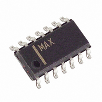
MAX4168ESD+ Maxim Integrated Products, MAX4168ESD+ Datasheet - Page 10

MAX4168ESD+
Manufacturer Part Number
MAX4168ESD+
Description
IC OP AMP R-R I/O W/SD 14-SOIC
Manufacturer
Maxim Integrated Products
Datasheet
1.MAX4166ELAT.pdf
(17 pages)
Specifications of MAX4168ESD+
Amplifier Type
General Purpose
Number Of Circuits
2
Output Type
Rail-to-Rail
Slew Rate
2 V/µs
Gain Bandwidth Product
5MHz
Current - Input Bias
50nA
Voltage - Input Offset
250µV
Current - Supply
1.3mA
Current - Output / Channel
125mA
Voltage - Supply, Single/dual (±)
2.7 V ~ 6.5 V, ±1.35 V ~ 3.25 V
Operating Temperature
-40°C ~ 85°C
Mounting Type
Surface Mount
Package / Case
14-SOIC (3.9mm Width), 14-SOL
Number Of Channels
2
Voltage Gain Db
120 dB
Common Mode Rejection Ratio (min)
72 dB
Input Offset Voltage
0.85 mV
Operating Supply Voltage
3 V, 5 V
Maximum Power Dissipation
667 mW
Maximum Operating Temperature
+ 85 C
Mounting Style
SMD/SMT
Maximum Dual Supply Voltage
+/- 3.25 V
Minimum Operating Temperature
- 40 C
Lead Free Status / RoHS Status
Lead free / RoHS Compliant
-3db Bandwidth
-
Lead Free Status / Rohs Status
Details
High-Output-Drive, Precision, Low-Power, Single-
Supply, Rail-to-Rail I/O Op Amps with Shutdown
Figure 3. Dual MAX4167/MAX4168 Bridge Amplifier for
200mW at 3V
The MAX4165/MAX4166 can be used as a single-sup-
ply speaker driver, as shown in the Typical Operating
Circuit . Capacitor C1 is used for blocking DC (a 0.1µF
ceramic capacitor can be used). When choosing resis-
tors R3 and R4, take into consideration the input bias
current as well as how much supply current can be tol-
erated. Choose resistors R1 and R2 according to the
amount of gain and current desired. Capacitor C3
ensures unity gain for DC. A 10µF electrolytic capacitor
is suitable for most applications. The coupling capaci-
tor C2 sets a low-frequency pole and is fairly large in
value. For a 32Ω load, a 100µF coupling capacitor
gives a low-frequency pole at 50Hz. The low-frequency
pole can be set according to the following equation:
The circuit shown in Figure 3 uses a dual MAX4167/
MAX4168 to implement a 3V, 200mW amplifier suitable
for use in size-constrained applications. This configura-
tion eliminates the need for the large coupling capaci-
tor required by the single op-amp speaker driver when
single-supply operation is a must. Voltage gain is set to
+10V/V; however, it can be changed by adjusting the
900kΩ resistor value. DC voltage at the speaker is limit-
ed to 10mV. The 47Ω and 0.1µF capacitors across the
speaker maintain a low impedance at the load as fre-
quency increases.
10
0.25Vp-p
INPUT
______________________________________________________________________________________
0.1 F
100k
4.7k
V
CC
100k
100k
= +3V
4.7k
Single-Supply Speaker Driver
= 1 / 2 (R
1/2 MAX4167
1/2 MAX4168
1 F
100k
100k
100k
V
CC
= +3V
L
C2)
1/2 MAX4167
1/2 MAX4168
Bridge Amplifier
900k
0.1 F
V
47
CC
= +3V
32
Devices in the MAX4165–MAX4169 family of high-out-
put-current amplifiers have rail-to-rail input and output
stages designed for low-voltage, single-supply opera-
tion. The input stage consists of separate NPN and
PNP differential stages that combine to provide an
input common-mode range that extends 0.25V beyond
the supply rails. The PNP stage is active for input volt-
ages close to the negative rail, and the NPN stage is
active for input voltages near the positive rail. The
switchover transition region, which occurs near V
has been extended to minimize the slight degradation
in common-mode rejection ratio caused by mismatch of
the input pairs.
Figure 4. Reducing Offset Error Due to Bias Current
(Noninverting)
Figure 5. Reducing Offset Error Due to Bias Current (Inverting)
R3 = R1
R3 = R1
R2
R2
R3
R1
R3
R1
Rail-to-Rail Input Stage
R2
R2
MAX4165
MAX4166
MAX4167
MAX4168
MAX4169
MAX4165
MAX4166
MAX4167
MAX4168
MAX4169
CC
/ 2,


