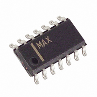
MAX4168ESD+ Maxim Integrated Products, MAX4168ESD+ Datasheet - Page 12

MAX4168ESD+
Manufacturer Part Number
MAX4168ESD+
Description
IC OP AMP R-R I/O W/SD 14-SOIC
Manufacturer
Maxim Integrated Products
Datasheet
1.MAX4166ELAT.pdf
(17 pages)
Specifications of MAX4168ESD+
Amplifier Type
General Purpose
Number Of Circuits
2
Output Type
Rail-to-Rail
Slew Rate
2 V/µs
Gain Bandwidth Product
5MHz
Current - Input Bias
50nA
Voltage - Input Offset
250µV
Current - Supply
1.3mA
Current - Output / Channel
125mA
Voltage - Supply, Single/dual (±)
2.7 V ~ 6.5 V, ±1.35 V ~ 3.25 V
Operating Temperature
-40°C ~ 85°C
Mounting Type
Surface Mount
Package / Case
14-SOIC (3.9mm Width), 14-SOL
Number Of Channels
2
Voltage Gain Db
120 dB
Common Mode Rejection Ratio (min)
72 dB
Input Offset Voltage
0.85 mV
Operating Supply Voltage
3 V, 5 V
Maximum Power Dissipation
667 mW
Maximum Operating Temperature
+ 85 C
Mounting Style
SMD/SMT
Maximum Dual Supply Voltage
+/- 3.25 V
Minimum Operating Temperature
- 40 C
Lead Free Status / RoHS Status
Lead free / RoHS Compliant
-3db Bandwidth
-
Lead Free Status / Rohs Status
Details
High-Output-Drive, Precision, Low-Power, Single-
Supply, Rail-to-Rail I/O Op Amps with Shutdown
Figure 8. Capacitive - Load Stability
Figure 10. Small-Signal Transient Response with Excessive
Capacitive Load with Isolation Resistor
The MAX4166/MAX4168 have a shutdown option.
When the shutdown pin (SHDN) is pulled low, supply
current drops to 58µA per amplifier (V
amplifiers are disabled, and their outputs are placed in
a high-impedance state. Pulling SHDN high or leaving it
floating enables the amplifier. In the dual MAX4168, the
two amplifiers shut down independently. Figures 12
and 13 show the MAX4166’s output voltage and sup-
ply-current responses to a shutdown pulse. The
MAX4166–MAX4169 typically settle within 5µs after
power-up (Figure 14).
12
______________________________________________________________________________________
(20mV/div)
(20mV/div)
1300
1200
1100
1000
300
900
800
700
600
500
400
200
100
OUT
0
IN
10
Power-Up and Shutdown Modes
V
R
V
R
UNSTABLE REGION
CC
L
CC
L
to V
= 100k , R
= +5.0V
= +3.0V, C
CC
100
/ 2
RESISTIVE LOAD (k )
ISO
L
TIME (1 s/div)
= 1500pF
= 39
STABLE REGION
1k
10k
CC
= +5V), the
100k
The MAX4165–MAX4169 can operate from a single
+2.7V to +6.5V supply, or from dual ±1.35V to
±3.25V supplies. For single-supply operation, bypass
the power supply with a 0.1µF ceramic capacitor in
parallel with at least 1µF. For dual-supply operation,
bypass each supply to ground. Good layout improves
performance by decreasing the amount of stray capac-
itance at the op amps’ inputs and outputs. Decrease
stray capacitance by placing external components
close to the op amps’ pins, minimizing trace and lead
lengths.
Figure 9. Small-Signal Transient Response with Excessive
Capacitive Load
Figure 11. Capacitive-Load-Driving Circuit
(20mV/div)
(20mV/div)
OUT
IN
V
R
CC
L
= 100k , R
= +3.0V, C
Power Supplies and Layout
ISO
L
TIME (1 s/div)
= 1500pF
= 0
R
ISO
C
L


